Supercharge Your Innovation With Domain-Expert AI Agents!

Epitaxy base, semiconductor light emitting device and manufacturing methods thereof

a light-emitting device and semiconductor technology, applied in the direction of polycrystalline material growth, crystal growth process, chemically reactive gas, etc., can solve the problems of increased chance of crack generation and severe bent of light-emitting device, and achieve the effect of improving working efficiency and preferable epitaxy quality

Active Publication Date: 2016-08-23
PLAYNITRIDE
View PDF6 Cites 0 Cited by
  • Summary
  • Abstract
  • Description
  • Claims
  • Application Information

AI Technical Summary

Benefits of technology

The invention is a method for manufacturing an epitaxy base and a semiconductor light emitting device. By using a specific process for forming a nucleating layer on a substrate, the subsequent growth of semiconductor layers results in a higher quality epitaxy and better working efficiency of the device. The nucleating layer is made of a single crystal aluminum nitride layer that has a well-organized lattice structure. This ensures a more favorable growth of semiconductor layers and improves the overall quality of the semiconductor light emitting device.

Problems solved by technology

Therefore, the conventional semiconductor light emitting device may be severely bent due to the stress and the chance of generating cracks is thus increased.

Method used


Image

  • Epitaxy base, semiconductor light emitting device and manufacturing methods thereof
  • Epitaxy base, semiconductor light emitting device and manufacturing methods thereof
  • Epitaxy base, semiconductor light emitting device and manufacturing methods thereof

Examples


Embodiment Construction

[0031]Reference will now be made in detail to the present preferred embodiments of the invention, examples of which are illustrated in the accompanying drawings. Wherever possible, the same reference numbers are used in the drawings and the description to refer to the same or like parts.

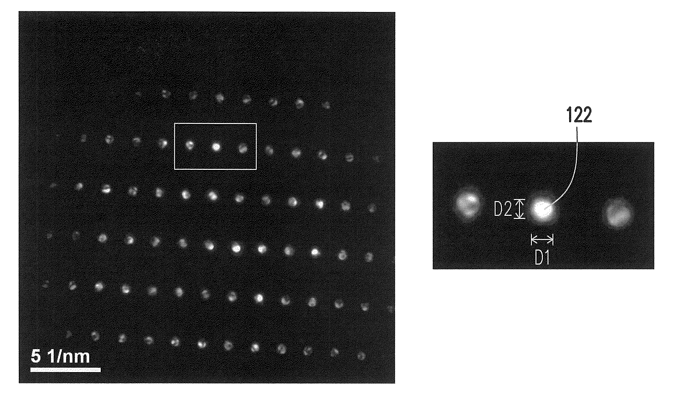
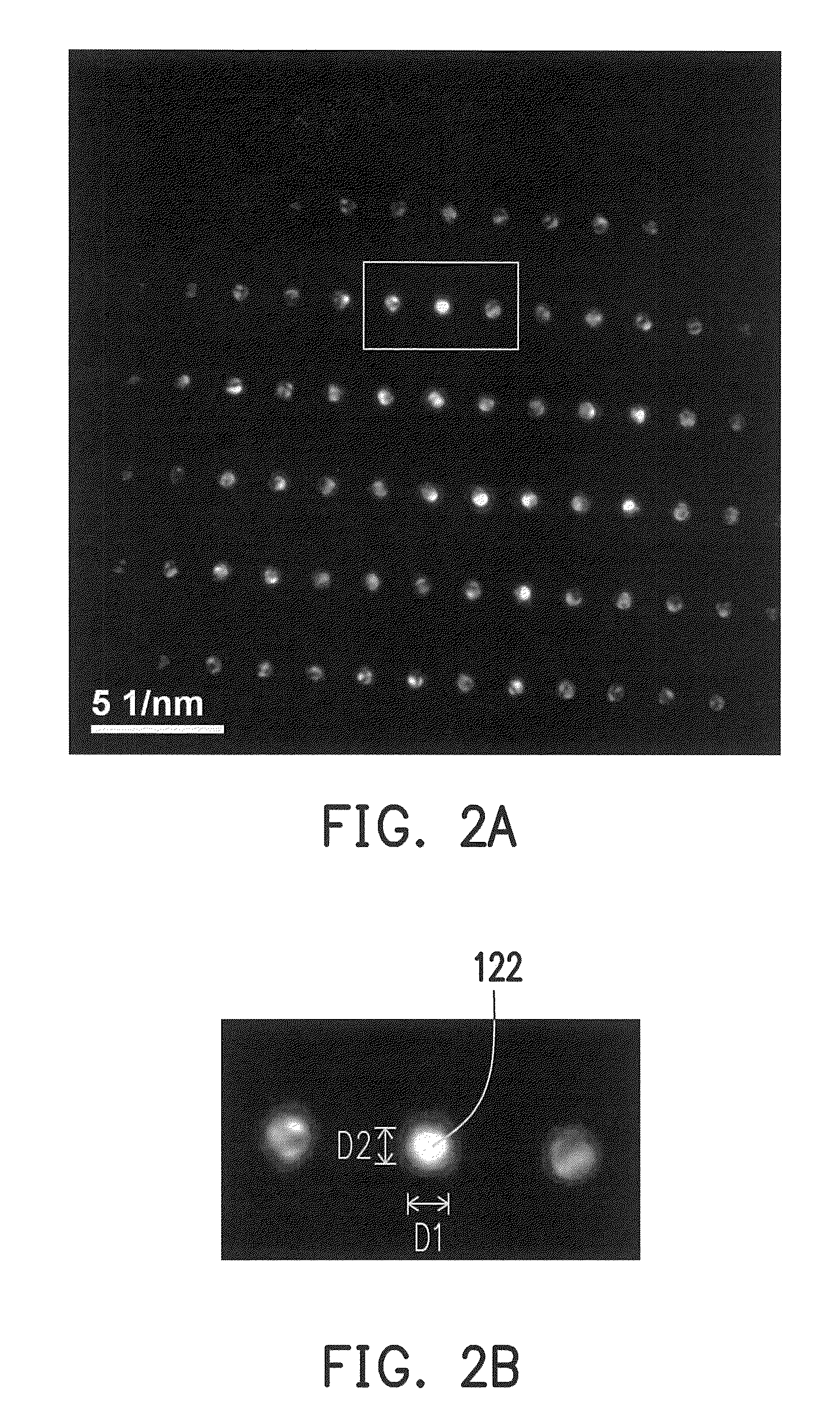
[0032]FIG. 1 is a schematic view illustrating an epitaxy base according to an embodiment of the invention. Referring to FIG. 1, an epitaxy base 100 of this embodiment includes a substrate 110 and a nucleating layer 120.

[0033]In this embodiment, the substrate 110 is a sapphire substrate. However, in other embodiments, any substrate material capable of growing a Group III-V (e.g. a Group III nitride) semiconductor layer, such as Si, SiO2, GaN, AlN, spinnel, SiC, GaAs, LiGaO2, LiAlO2, or MgAl2O4, for example, may be used.

[0034]As shown in FIG. 1, in this embodiment, the nucleating layer 120 is directly disposed on a surface of the substrate 110, and the surface where the substrate 110 contacts the nucle...


PUM

PropertyMeasurementUnit
crystal structureaaaaaaaaaa
lengthsaaaaaaaaaa
diametersaaaaaaaaaa

Abstract

An epitaxy base including a substrate and a nucleating layer disposed on the substrate. The nucleating layer is an AlN layer with a single crystal structure. A diffraction pattern of the nucleating layer includes a plurality of dot patterns. Each of the dot patterns is substantially circular, and a ratio between lengths of any two diameters perpendicular to each other on each of the dot patterns ranges from approximately 0.9 to approximately 1.1. A semiconductor light emitting device, a manufacturing method of the epitaxy base, and a manufacturing method of the light emitting semiconductor device are further provided.

Description

CROSS-REFERENCE TO RELATED APPLICATION[0001]This application claims the priority benefit of Taiwan application serial no. 103134381, filed on Oct. 2, 2014. The entirety of the above-mentioned patent application is hereby incorporated by reference herein and made a part of this specification.BACKGROUND OF THE INVENTION[0002]1. Field of the Invention[0003]The invention relates to an epitaxy base, a semiconductor light emitting device, and manufacturing methods thereof, and particularly relates to an epitaxy base, a semiconductor light emitting device, and manufacturing methods thereof offering a preferable epitaxy quality.[0004]2. Description of Related Art[0005]Semiconductor light emitting devices, such as light-emitting diodes (LEDs), are manufactured by using compounds (e.g. gallium nitride, gallium phosphide, and gallium arsenide.) containing a Group III-V element. A lifetime of the LEDs may be as long as 100,000 hours. In addition, the LEDs have the advantages of a quick respondi...

Claims


Application Information

Patent Timeline
Patent Type & Authority Patents(United States)
IPC IPC(8): H01L21/00H01L31/109H01L33/12H01L27/15H01L21/20H01L33/58C23C14/34H01L33/32H01L33/00
CPCH01L33/12H01L33/58H01L33/0075H01L33/32C23C14/34C30B25/183C30B29/403C30B23/00H01L21/0242H01L21/02458H01L21/0254H01L33/007C30B23/08C30B29/406
Inventor LAI, YEN-LINWU, JYUN-DE
Owner PLAYNITRIDE
Features
  • R&D
  • Intellectual Property
  • Life Sciences
  • Materials
  • Tech Scout
  • Unparalleled Data Quality
  • Higher Quality Content
  • 60% Fewer Hallucinations
Learn More