Optically powered and controlled non-foster circuit

a non-foster circuit, optically powered technology, applied in the direction of impedence convertors, electrical devices, antennas, etc., can solve the problems of limited performance, inability to maintain bright lines of distinction between these terms, and the stability margin typically approaching zero

Active Publication Date: 2016-08-23
HRL LAB
View PDF72 Cites 8 Cited by
  • Summary
  • Abstract
  • Description
  • Claims
  • Application Information

AI Technical Summary

Problems solved by technology

AMC, AIS and FSS are all well known in the art and look very similar to each other which means that persons skilled in the art have not always maintained bright lines of distinction between these terms.
Therefore, the performance is limited by the fundamental bandwidth-efficiency tradeoff given by the Chu limit when passive matching is employed.
The main challenge in realizing NFCs is stability; NICs and NIIs are conditionally stable, and the stability margin typically approaches zero as immittance cancellation becomes more complete.
One issue with the use of NFCs in these arrays is that the power and control wiring to the NFCs can affect the electromagnetic properties of an active AIS system.
Furthermore, it can be challenging to run the wires over a distance more than about an inch.
Most importantly, this approach does not extend to bulk metamaterials or metasurfaces with no ground plane.
However, batteries are large so that integration into smaller areas such as 1 square millimeter is not practical.
In addition, batteries are heavy and are not practical in extreme temperatures and in high shock applications.
More importantly, a battery powered NFC cannot be controlled remotely, either to turn it on / off or to vary the circuit parameters.
Furthermore, it would be undesirable for an operator to control NFCs manually in an array / AIS environment which may have hundreds of NFCs.

Method used


Image

  • Optically powered and controlled non-foster circuit
  • Optically powered and controlled non-foster circuit
  • Optically powered and controlled non-foster circuit

Examples


Embodiment Construction

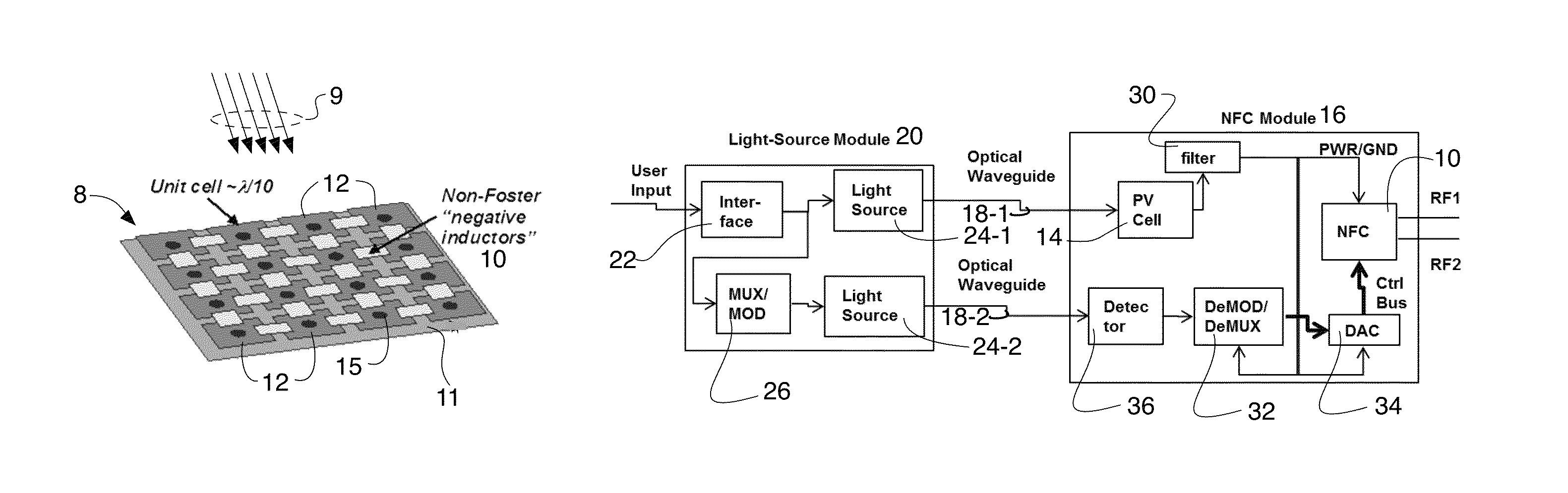
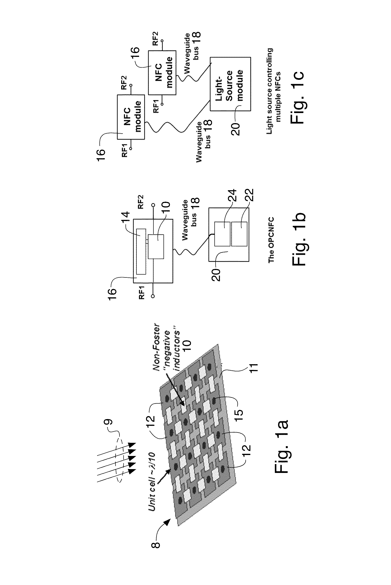
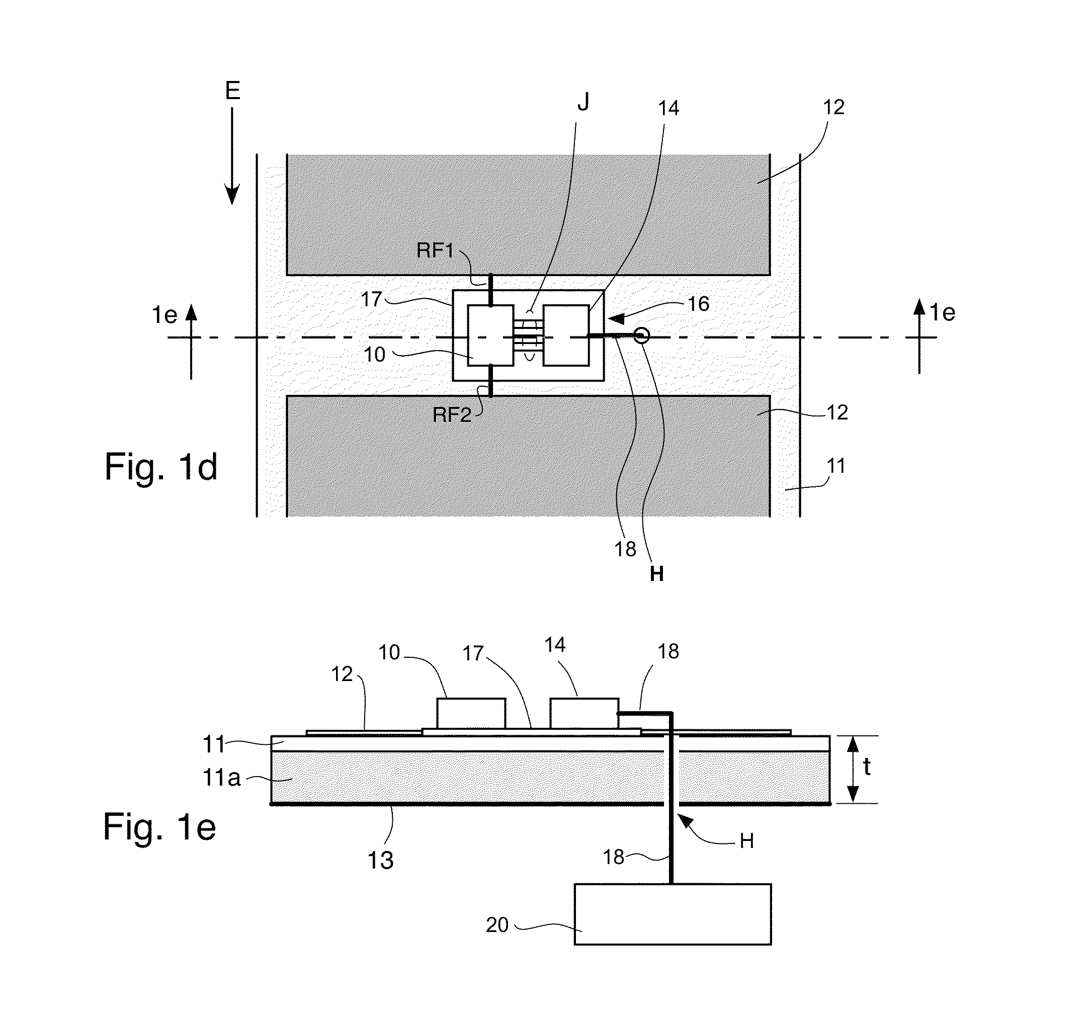
[0027]An exemplary application of OPCNFCs is the Active Artificial Impedance Surface (AAIS) 8 of FIG. 1a in which NFCs 10 which are preferably set up to serve as negative inductors (see, for example, FIG. 2) are connected between patches 12 which are arranged in a subwavelength periodic grid (which may have a pitch—or a spacing between centers thereof—equal to about λ / 10 where λ is the wavelength of impinging electromagnetic (EM) radiation 9 with which the AAIS is meant to interact). The patches 12 of FIG. 1a are depicted as square shaped but those skilled in the art making Artificial Impedance Surfaces know that the patches 12 may assume other geometric shapes (such as triangular shaped patches, hexagonal shaped patches, rectangular shaped patches, etc.). The patches 12 are disposed on a dielectric substrate 11 and are typically (but not necessarily) coupled to a ground plane 13 (disposed on an opposing surfaces of the dielectric substrate 11—see FIG. 1e) by a centrally located met...


PUM


Abstract

This invention is the Optically Powered and Controlled Non-Foster Circuit (OPCNFC) that is electrically floating; i.e., it does not have any metallic electrical / conductive connection to a power supply, ground, or control signal. Rather power and control signals are applied to the OPCNFC using optical energy. The Non-Foster Circuit (NFC) synthesizes negative inductance, negative capacitance, and / or negative resistance between metallic patches disposed in an array of an Artificial Impedance Surface (AIS).

Description

CROSS REFERENCE TO RELATED APPLICATIONS[0001]This application is related to the following U.S. patent applications: (i) U.S. patent application Ser. No. 13 / 441,659,” entitled “Wideband Tunable Impedance Surfaces” filed Apr. 4, 2012, (ii) U.S. Provisional Patent Application Ser. No. 61 / 537,488 entitled “Wideband Tunable Impedance Surfaces”, filed Sep. 21, 2011; (iii) U.S. Provisional Patent Application Ser. No. 61 / 473,076 entitled “Wideband Adaptable Artificial Impedance Surface”, filed Apr. 7, 2011; (iv) U.S. Provisional Patent Application Ser. No. 61 / 505,037 entitled “Differential Negative Impedance Converters and Inverters with Tunable Conversion Ratios” filed Jul. 6, 2011; (v) U.S. patent application Ser. No. 12 / 768,563 entitled “Non-Foster Impedance Power Amplifier”, filed Apr. 27, 2010; and (vi) U.S. patent application Ser. No. 13 / 441,730 entitled “Differential Negative Impedance Converters and Inverters with Tunable Conversion Ratios”, filed Apr. 6, 2012, each of which is here...

Claims


Application Information

Patent Timeline
Patent Type & Authority Patents(United States)
IPC IPC(8): H03H11/44H03H11/28
CPCH03H11/44H03H11/28H02J50/30H01Q15/0066H01Q15/008
Inventor WHITE, CARSON R.SCHAFFNER, JAMES H.
Owner HRL LAB
Why Eureka
Try Eureka