Display device

a technology of display device and thin film, which is applied in the direction of identification means, sustainable manufacturing/processing, instruments, etc., can solve the problems of patent document 1 not revealing a material, too soft for the transfer of thin film device layer, and low power consumption, and achieve high reliability.

Active Publication Date: 2016-08-30
SEMICON ENERGY LAB CO LTD
View PDF12 Cites 24 Cited by
  • Summary
  • Abstract
  • Description
  • Claims
  • Application Information

AI Technical Summary

Benefits of technology

[0012]Another object of one embodiment of the present invention is to provide a highly reliable display device, electronic device, or lighting device.
[0013]Another object of one embodiment of the present invention is to provide a display device, electronic device, or lighting device that is unlikely to be broken.
[0014]Another object of one embodiment of the present invention is to provide a display device, electronic device, or lighting device with low power consumption.
[0023]In one embodiment of the present invention, a highly reliable display device, electronic device, or lighting device can be provided.
[0025]In one embodiment of the present invention, a display device, electronic device, or lighting device with low power consumption can be provided.

Problems solved by technology

In Patent Document 1, materials of the plastic substrate that can be used for a display device are listed; however, some of them, such as a fluorine rubber material or a silicone resin, are too soft to be favorable for transfer of a thin film device layer.
Furthermore, Patent Document 1 does not disclose a material for a substrate that can be favorably used in a repeatedly bendable display device.

Method used


Image

  • Display device
  • Display device
  • Display device

Examples


embodiment 1

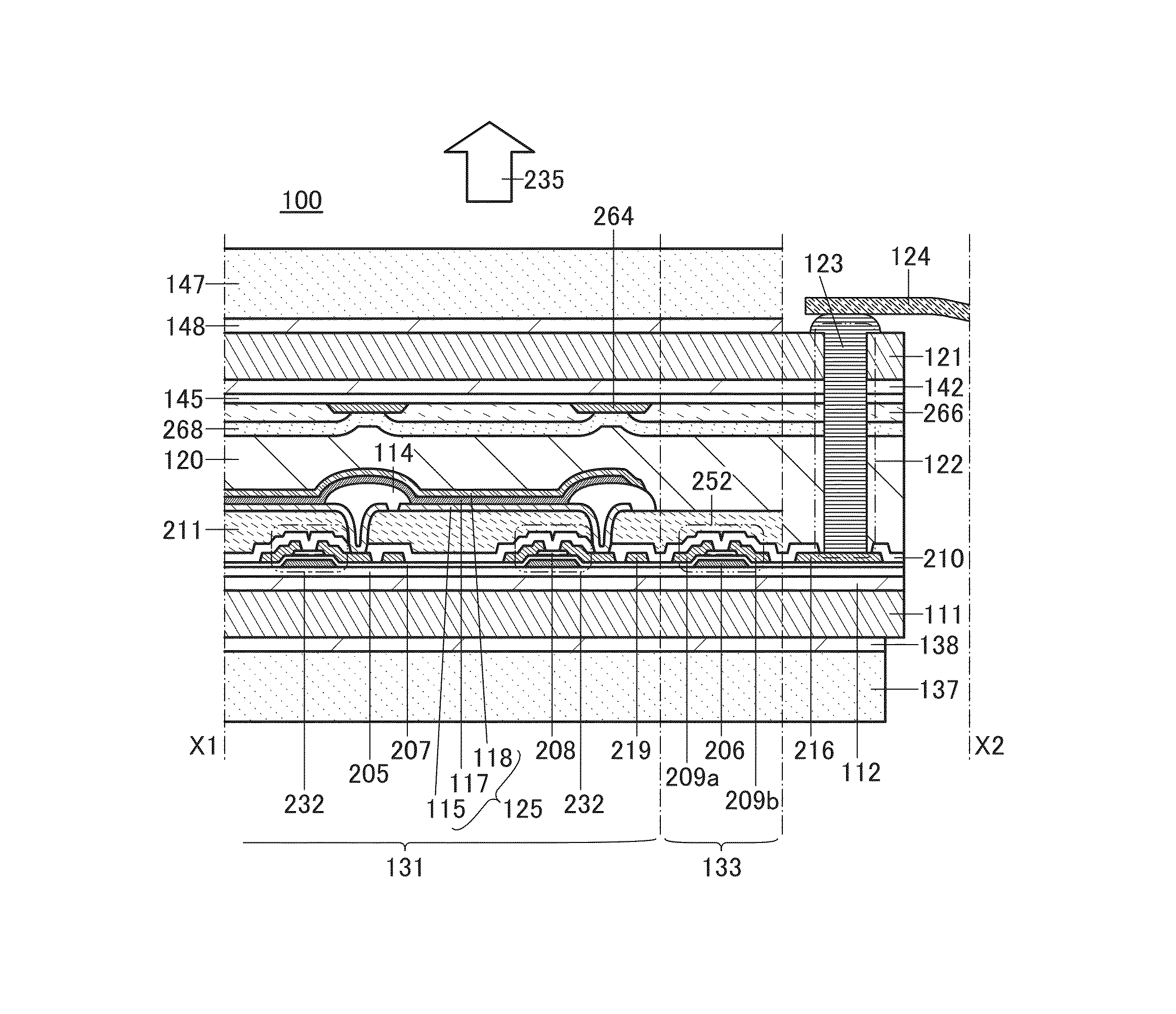
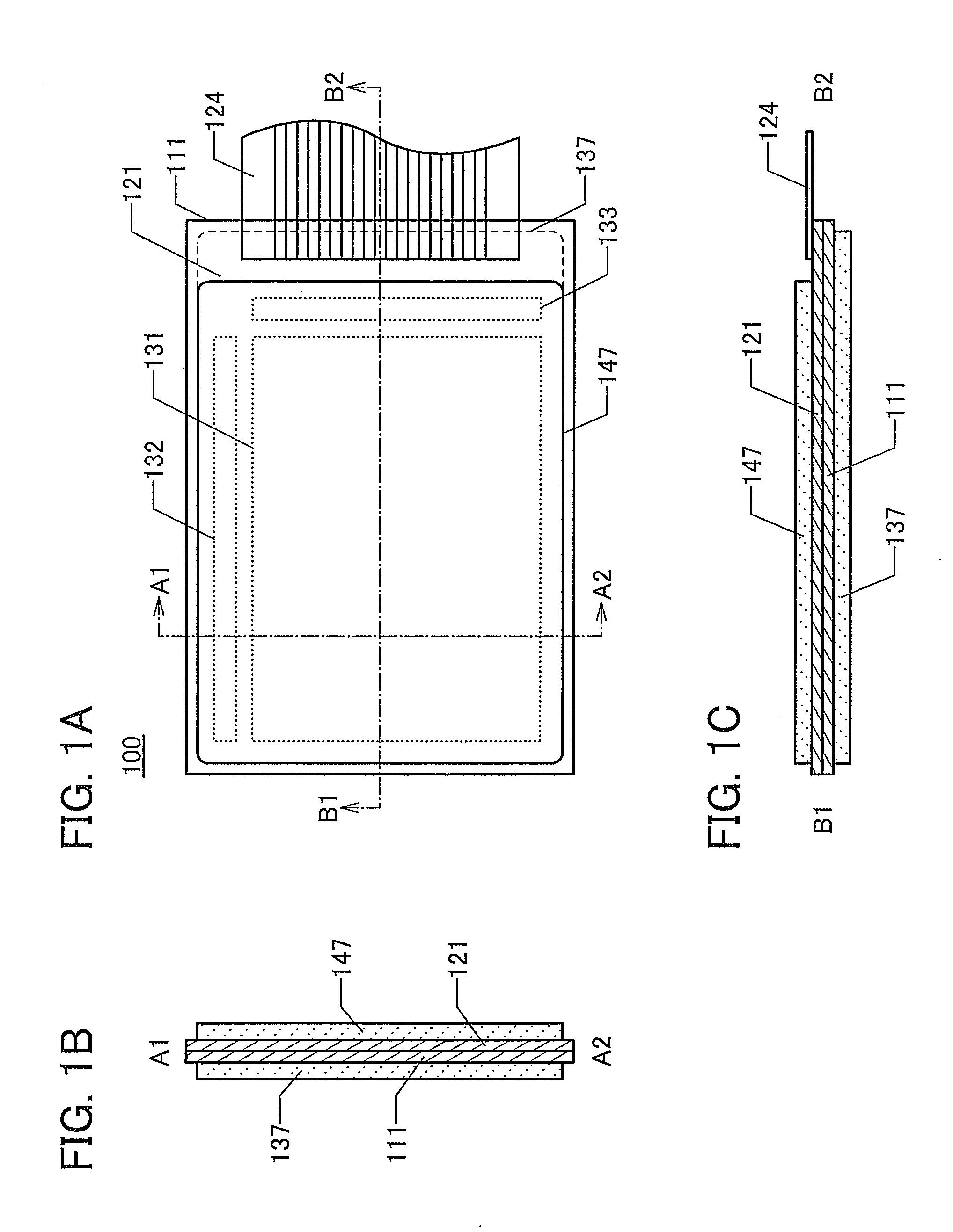
[0067]A structure example of a display device 100 that is one embodiment of the present invention will be described with reference to drawings. FIG. 1A is a top view of the display device 100 and FIG. 1B is a cross-sectional view taken along a dashed-dotted line A1-A2 in FIG. 1A. FIG. 1C is a cross-sectional view taken along a dashed-dotted line B1-B2 in FIG. 1A.

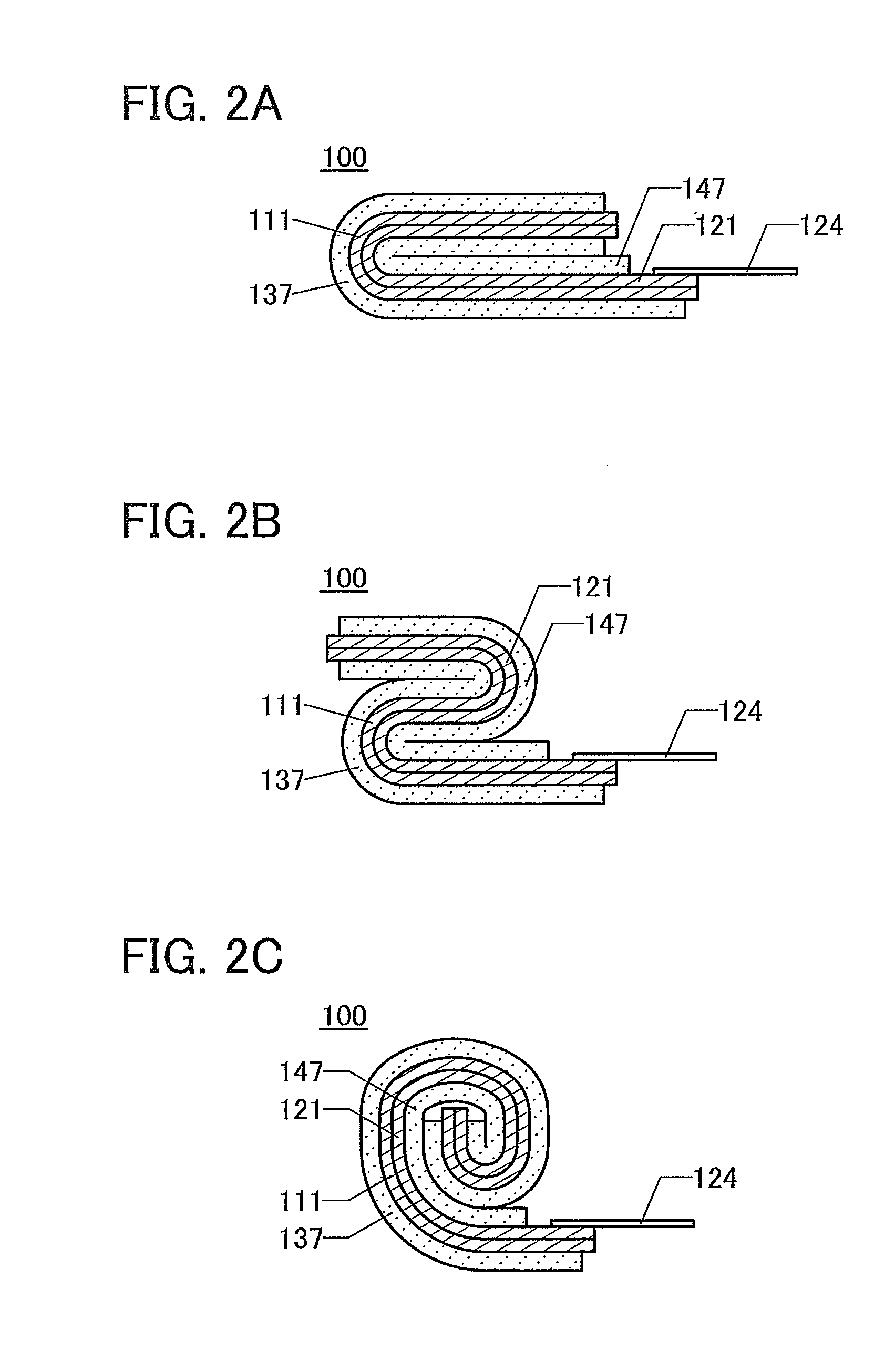
[0068]The cross-sectional structure of one embodiment of the present invention is not limited to that illustrated in FIG. 1C. For example, any of cross-sectional structures illustrated in FIGS. 24A to 24F may also be employed. The external electrode 124 may be covered with a substrate 147 as illustrated in FIGS. 24B, 24C, and 24F, in which case a connection portion can be protected. Note that FIGS. 24D to 24F each illustrate a structure in which a semiconductor chip 910 is provided over a substrate by COG or the like. When the semiconductor chip 910 is covered with the substrate 147 as illustrated in FIGS. 24E and 24F, the s...

modification example

[0123]FIGS. 5A to 5C illustrate a display device 200 having a structure different from that of the display device 100. FIG. 5A is a top view of the display device 200 and FIG. 5B is a cross-sectional view taken along a dashed-dotted line A3-A4 in FIG. 5A. FIG. 5C is a cross-sectional view taken along a dashed-dotted line B3-B4 in FIG. 5A.

[0124]The cross-sectional structure of one embodiment of the present invention is not limited to that illustrated in FIG. 5C. For example, any of cross-sectional structures illustrated in FIGS. 26A to 26H may also be employed. The external electrode 124 may be covered with the substrate 147 as illustrated in FIGS. 26B, 26C, 26D, 26G, and 26H, in which case a connection portion can be protected. The external electrode 124 may be covered with the substrate 147 and the substrate 137 as illustrated in FIGS. 26D and 26H, in which case a connection portion can be protected. When the semiconductor chip 910 is covered with the substrate 147 as illustrated i...

embodiment 2

[0128]In this embodiment, another example of a method for manufacturing the display device 100 will be described with reference to FIGS. 6A to 6D, FIGS. 7A to 7D. FIGS. 8A and 8B, FIGS. 9A and 9B, FIGS. 10A and 10B, FIGS. 11A and 11B, and FIG. 12. Note that FIGS. 6A to 6D. FIGS. 7A to 7D, FIGS. 8A and 8B, FIGS. 9A and 9B, FIGS. 10A and 10B, FIGS. 11A and 11B, and FIG. 12 are each a cross-sectional view taken along a dashed-dotted line X1-X2 in FIG. 3A.

[Formation of Separation Layer]

[0129]First, a separation layer 113 is formed over an element formation substrate 101 (see FIG. 6A). Note that the element formation substrate 101 may be a glass substrate, a quartz substrate, a sapphire substrate, a ceramic substrate, a metal substrate, or the like. Alternatively, the element formation substrate 101 may be a plastic substrate having heat resistance to the processing temperature in this embodiment.

[0130]As the glass substrate, for example, a glass material such as aluminosilicate glass, a...


PUM

PropertyMeasurementUnit
Young's modulusaaaaaaaaaa

Abstract

A display device, an electronic device, or a lighting device that is unlikely to be broken is provided. A flexible first substrate and a flexible second substrate overlap with each other with a display element provided therebetween. A flexible third substrate is bonded on the outer surface of the first substrate, and a flexible fourth substrate is bonded on the outer surface of the second substrate. The third substrate is formed using a material softer than the first substrate, and the fourth substrate is formed using a material softer than the second substrate.

Description

BACKGROUND OF THE INVENTION[0001]1. Field of the Invention[0002]One embodiment of the present invention relates to an object, a method, or a manufacturing method. In addition, one embodiment of the present invention relates to a process, a machine, manufacture, or a composition of matter. One embodiment of the present invention particularly relates to a light-emitting device, a display device, an electronic device, a lighting device, a manufacturing method thereof, a usage method thereof, an operation method thereof, or the like. In particular, the present invention relates to a light-emitting device, a display device, an electronic device, or a lighting device utilizing electroluminescence (EL), a manufacturing method thereof, a usage method thereof, an operation method thereof, or the like.[0003]2. Description of the Related Art[0004]Recent light-emitting devices and display devices are expected to be applied to a variety of uses and become diversified.[0005]For example, light-emi...

Claims


Application Information

Patent Timeline
Patent Type & Authority Patents(United States)
IPC IPC(8): C09K19/00H01L51/00
CPCH01L51/0097H01L2251/5338Y02P70/521H01L2251/55Y02E10/549Y10T428/10Y10T428/1086C09K2323/06C09K2323/00Y02P70/50H10K77/111H10K2101/00H10K2102/311G09F9/301G09F9/33H10K59/123H10K71/50H10K59/60H10K50/84H10K59/12H10K59/40H10K71/00H10K59/1201H10K2102/3026H10K2102/3035G06F1/1652
Inventor KAWATA, TAKUYACHIDA, AKIHIRO
Owner SEMICON ENERGY LAB CO LTD
Why Eureka
Try Eureka