Diamond single crystal, method for producing the same, and single crystal diamond tool

a diamond single crystal and diamond tool technology, applied in the field of diamond single crystal, method for producing the same, and single crystal diamond tool, can solve the problems of fluctuation in the price and factor contrary to stable supply, increase or decrease in the amount of commercial natural diamond single crystals, etc., to achieve high hardness, high toughness, and easy processing

Active Publication Date: 2016-09-13
SUMITOMO ELECTRIC IND LTD
View PDF27 Cites 2 Cited by
  • Summary
  • Abstract
  • Description
  • Claims
  • Application Information

AI Technical Summary

Benefits of technology

[0020]The present invention can provide a diamond single crystal that has high hardness and high toughness, is easy to process in the manufacture of a tool, has cracking or chipping resistance equal to or higher than the cracking or chipping resistance of tools that include natural diamonds or high-temperature and high-pressure synthesized Ib diamonds, and has long life and high fracture resistance in cutting, a single crystal diamond tool, and a method for producing the diamond single crystal.

Problems solved by technology

Fluctuation in the price and amount of commercial natural diamond single crystals, which account for most of the industrial diamonds, is a factor contrary to stable supply.
A decrease in the reserve of natural diamonds may cause an increase in price or a decrease in the amount of commercial natural diamond single crystals.
However, in industrial applications, particularly in cutting tool applications, existing CVD diamond single crystals are not as widespread as high-pressure synthesized diamond single crystals.
This is because CVD diamond single crystals have lower toughness than natural diamond single crystals and high-temperature and high-pressure synthesized Ib-type diamond single crystals, and there is the technical problem that CVD diamond single crystals are difficult to process into the shape of a tool, such as a bit or an end mill, or chips or cracks tend to form during processing of a workpiece.
This is similar to the situation where high-temperature and high-pressure synthesized IIa-type diamond single crystals, which are relatively brittle because of a small amount of nitrogen impurity in the crystals as compared with high-temperature and high-pressure synthesized Ib-type diamond single crystals, are rarely used in cutting tool applications in spite of their possibilities of relatively high hardness and long life.

Method used


Image

  • Diamond single crystal, method for producing the same, and single crystal diamond tool
  • Diamond single crystal, method for producing the same, and single crystal diamond tool

Examples


example 1-1

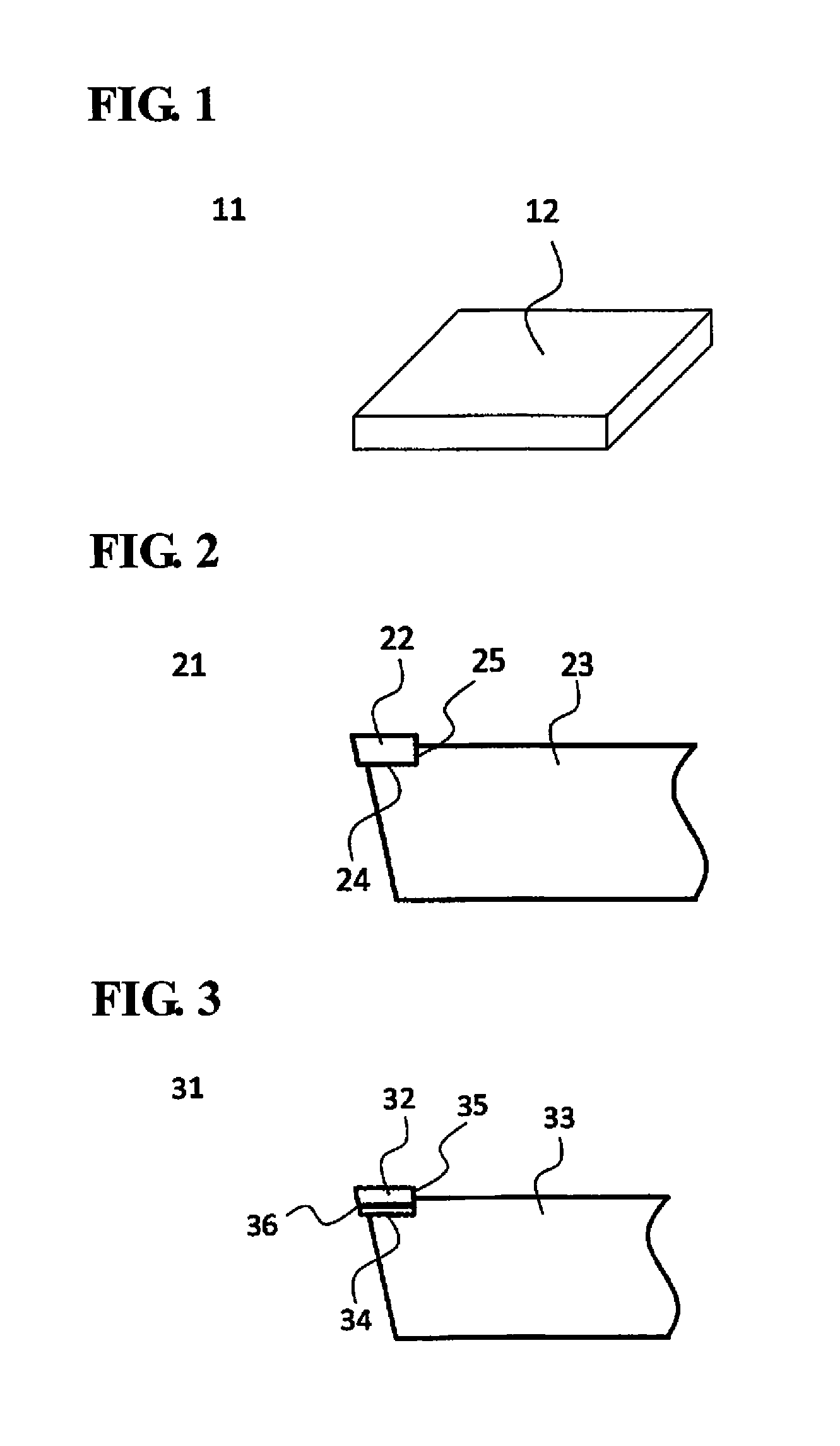
[0147]First, diamond single crystal seed substrates Nos. 1-01 to 1-22 listed in Table I were prepared. Each of these diamond single crystal seed substrates had a size of 4×4×0.5 mm in thickness. Nos. 1-01 to 1-13 were high-temperature and high-pressure synthesized Ib-type diamond single crystal substrates (HPHT Ib). Nos. 1-14 to 1-17 were high-temperature and high-pressure synthesized IIa-type diamond single crystal substrates (HPHT IIa). Nos. 1-18 to 1-22 were gas-phase-synthesized diamond single crystal substrates (CVD).

[0148]A 4×4 mm main surface ({100} plane) had a surface roughness Ra of 40 nm or less. Table I shows the off-angle of a main surface of each of the seed substrates on which a diamond single crystal is to be grown in a downstream process, and the transmittance of light having a wavelength of 800 nm.

[0149]The transmittance of light having a wavelength of 800 nm through each of the seed substrates was then decreased as shown in Table I by ion implantation through the ...

example 2-1

[0173]First, diamond single crystal seed substrates Nos. 2-01 to 2-22 listed in Table III were prepared. Each of these diamond single crystal seed substrates had a size of 4×4×0.5 mm in thickness. Nos. 2-01 to 2-13 were high-temperature and high-pressure synthesized Ib-type diamond single crystals (HPHT Ib). Nos. 2-14 to 2-17 were high-temperature and high-pressure synthesized IIa-type diamond single crystals (HPHT IIa). Nos. 2-18 to 2-22 were gas-phase-synthesized diamond single crystals (CVD).

[0174]A 4×4 mm main surface ({100} plane) had a surface roughness Ra of 40 nm or less. Table III shows the off-angle of a main surface of each of the seed substrates on which a diamond single crystal is to be grown in a downstream process, and the transmittance of light having a wavelength of 800 nm.

[0175]The transmittance of light having a wavelength of 800 nm through each of the seed substrates was then decreased as shown in Table III by ion implantation through the main surface. With respe...

example 2-2

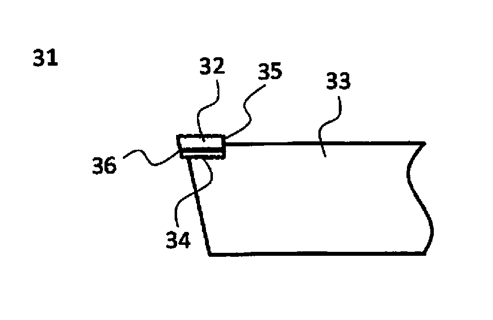
[0188]First, a diamond single crystal seed substrate No. 2-23 listed in Table V was prepared. The diamond single crystal seed substrate had a size of 4×4×0.5 mm in thickness and was a high-temperature and high-pressure synthesized Ib-type diamond single crystal (HPHT Ib). A 4×4 mm main surface had a surface roughness Ra of 40 nm or less. Table V shows the off-angle of a main surface of the seed substrate on which a diamond single crystal is to be grown in a downstream process, and the transmittance of light having a wavelength of 800 nm.

[0189]The transmittance of light having a wavelength of 800 nm through the seed substrate was then decreased as shown in Table V by ion implantation through the main surface. With respect to the ion implantation conditions, phosphorus was used as an ionic species, the implantation energy was 600 keV, and the implantation dose was 5×1015 cm−2. A diamond single crystal was epitaxially grown on the ion-implanted main surface.

[0190]A microwave plasma CVD...


PUM

PropertyMeasurementUnit
absorption coefficientaaaaaaaaaa

Abstract

A method for producing a diamond single crystal includes implanting an ion other than carbon into a surface of a diamond single crystal seed substrate and thereby decreasing the transmittance of light having a wavelength of 800 nm, the surface having an off-angle of 7 degrees or less with respect to a {100} plane, and homoepitaxially growing a diamond single crystal on the ion-implanted surface of the seed substrate using a chemical vapor synthesis under synthesis conditions where the ratio NC / NH of the number of carbon-containing molecules NC to the number of hydrogen molecules NH in a gas phase is 10% or more and 40% or less, the ratio NN / NC of the number of nitrogen molecules NN to the number of carbon-containing molecules NC in the gas phase is 0.1% or more and 10% or less, and the seed substrate temperature T is 850° C. or more and less than 1000° C.

Description

CROSS-REFERENCE TO RELATED APPLICATIONS[0001]This U.S. National stage application claims priority under 35 U.S.C. §119(a) to Japanese Patent Application No. 2012-146444 filed in Japan on Jun. 29, 2012, Japanese Patent Application No. 2012-152485 filed in Japan on Jul. 6, 2012, and Japanese Patent Application No. 2012-152503, filed in Japan on Jul. 6, 2012. The entire contents of Japanese Patent Application No. 2012-146444, Japanese Patent Application No. 2012-152485 and Japanese Patent Application No. 2012-152503 are hereby incorporated herein by reference in their entirety.TECHNICAL FIELD[0002]The present invention relates to a diamond single crystal for use in cutting tools, abrasion-resistant tools, precision tools, heat-dissipating members, substrates for semiconductor devices, and optical components, a method for producing the diamond single crystal, and a single crystal diamond tool, particularly a single crystal diamond cutting tool, for use in turning of parts of automobiles...

Claims


Application Information

Patent Timeline
Patent Type & Authority Patents(United States)
IPC IPC(8): C30B29/04B23B27/14C30B25/20C30B25/18C30B30/00
CPCC30B25/186B23B27/148C30B25/20C30B29/04C30B30/00Y10T407/24Y10T428/30B23B2226/31C30B31/22
Inventor UEDA, AKIHIKONISHIBAYASHI, YOSHIKISUMIYA, HITOSHI
Owner SUMITOMO ELECTRIC IND LTD
Why Eureka
Try Eureka