Thin film transistor, method of manufacturing the same, display substrate and display apparatus

a thin film transistor and manufacturing method technology, applied in the field of display, can solve the problems of adversely affecting the development of a high-performance display apparatus, serious lowering of the thin film transistor performance, etc., and achieve the effects of shortening the transmission distance of carriers, reducing the length of channels, and small channel lengths

Active Publication Date: 2016-10-25
BOE TECH GRP CO LTD
View PDF7 Cites 0 Cited by
  • Summary
  • Abstract
  • Description
  • Claims
  • Application Information

AI Technical Summary

Benefits of technology

[0033]According to the above technical solutions, in the thin film transistor according to the present invention, two etching barrier layers are disposed and the property that the first etching barrier layer at a lower position has a greater etch rate than the second etching barrier layer at an upper position is utilized. Therefore, an etched portion of the first etching barrier layer having a greater etch rate is greater than an etched portion of the second etching barrier layer having a smaller etch rate. As a result, a tapered groove structure or a tapered via hole structure is formed in the first etching barrier layer and the second etching barrier layer, shortening a transmission distance of carriers between the source and the drain and thus decreasing a length of a channel of the thin film transistor. Because of the small length of the channel, a size of the thin film transistor can be reduced, an aperture ratio of a liquid crystal panel is increased, and energy consumption is reduced. In addition, because of the small length of the channel, a turn-on current of the thin film transistor can be increased, and a charging efficiency is raised, so that whole performance of the thin film transistor is greatly improved, thereby facilitating development of high-resolution products.

Problems solved by technology

However, the conventional oxide thin film transistor has a long channel and a small turn-on current, which seriously lowers performance of the thin film transistor and adversely affects development of a high-performance display apparatus.

Method used


Image

  • Thin film transistor, method of manufacturing the same, display substrate and display apparatus
  • Thin film transistor, method of manufacturing the same, display substrate and display apparatus
  • Thin film transistor, method of manufacturing the same, display substrate and display apparatus

Examples


Embodiment Construction

[0038]The object, technical solutions and advantages of the present invention will be apparent and more readily appreciated from the following description of embodiments taken in conjunction with the accompanying drawings.

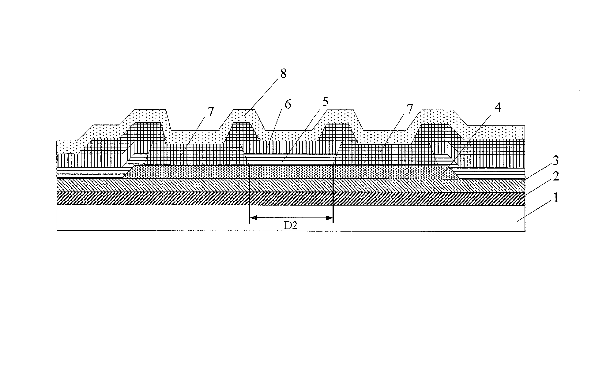
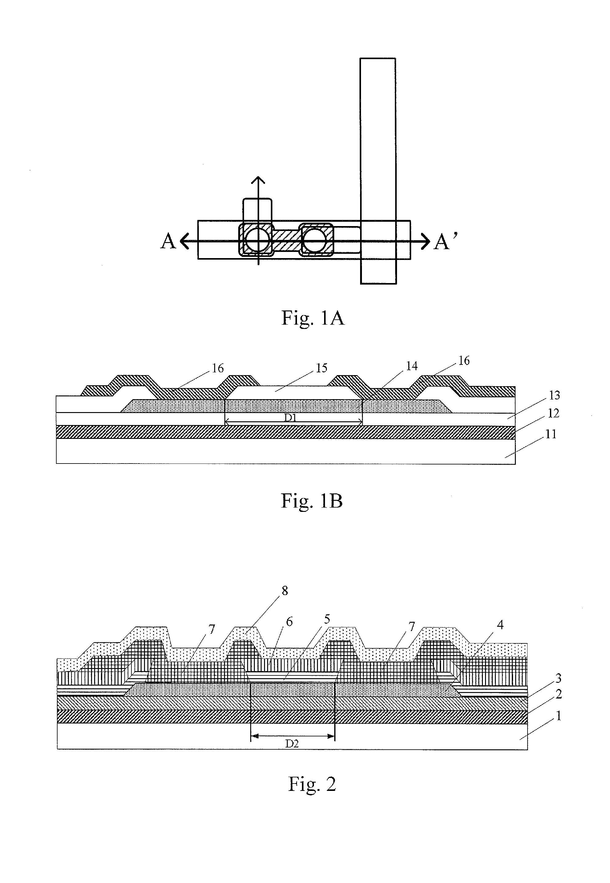
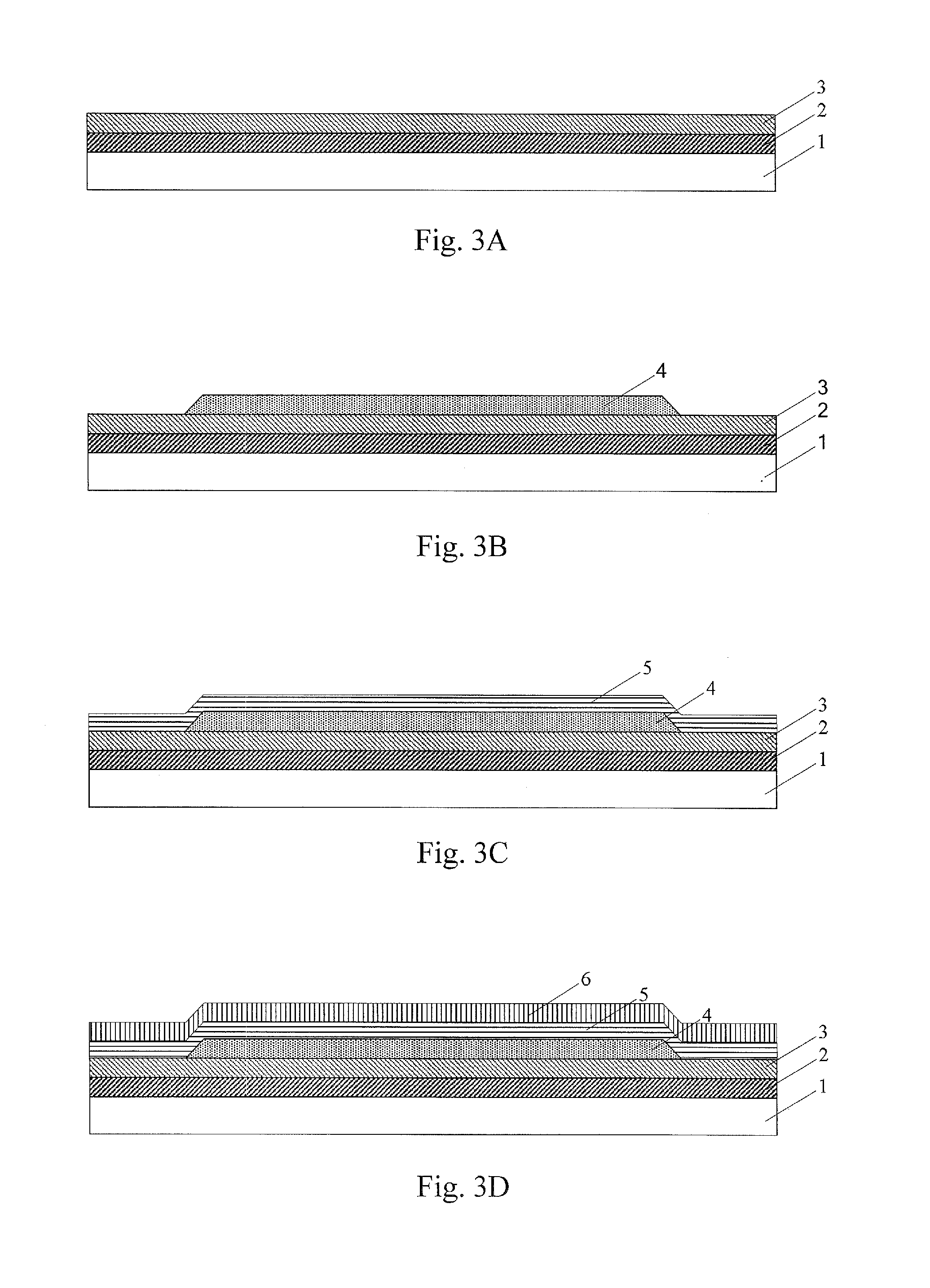
[0039]In accordance with an aspect of the present invention, there is provided a thin film transistor. As shown in FIG. 2, the thin film transistor comprises a substrate 1, an active layer 4, a first etching barrier layer 5, a second etching barrier layer 6, a source and a drain which are arranged in sequence, wherein:

[0040]the active layer 4 is disposed over the substrate 1;

[0041]the first etching barrier layer 5 is disposed over the active layer 4;

[0042]the second etching barrier layer 6 is disposed over the first etching barrier layer 5, and the first etching barrier layer 5 and the second etching barrier layer 6 are used to protect a portion of the active layer 4 in a channel region between the source and the drain from being corroded by a developing solution a...


PUM

PropertyMeasurementUnit
lengthaaaaaaaaaa
etch rateaaaaaaaaaa
deposition rateaaaaaaaaaa

Abstract

A thin film transistor is disclosed in the present invention. The thin film transistor comprises: a substrate, an active layer, a first etching barrier layer, a second etching barrier layer, a source and a drain, wherein: the active layer is disposed over the substrate; the first etching barrier layer is disposed over the active layer; the second etching barrier layer is disposed over the first etching barrier layer; the source and the drain are disposed over the second etching barrier layer, and are connected to each other through the active layer by means of via holes formed in the first etching barrier layer and the second etching barrier layer by etching; and a length of the first etching barrier layer at a channel position is less than a length of the second etching barrier layer. A method of manufacturing the thin film transistor, an array substrate and a display apparatus are also disclosed in the present invention. A length of a channel of the thin film transistor according to the present invention is less than the length of the channel of the conventional thin film transistor. Thereby, size and energy consumption of the thin film transistor are reduced, an aperture ratio of a liquid crystal panel is increased, and a turn-on current of the thin film transistor is increased, so that whole performance of the thin film transistor is further improved.

Description

CROSS-REFERENCE TO RELATED APPLICATION[0001]This application is a Section 371 National Stage Application of International Application No. PCT / CN2014 / 092362, filed 27 Nov. 2014, which claims the benefit of Chinese Patent Application No. 201410351335.8 filed on Jul. 22, 2014 in the State Intellectual Property Office of China, the whole disclosure of which is incorporated herein by reference.BACKGROUND[0002]1. Technical Field[0003]The present invention relates to the field of display, and particularly to a Thin Film Transistor (TFT), a method of manufacturing the same, a display substrate and a display apparatus.[0004]2. Description of the Related Art[0005]FIG. 1A is a schematic structural view of a conventional etching barrier type oxide thin film transistor, and FIG. 1B is a sectional view of the oxide thin film transistor shown in FIG. 1A, which is taken along the line A-A′ in FIG. 1A. As shown in FIGS. 1A and 1B, 11 denotes a substrate, 12 denotes a gate, 13 denotes a gate insulati...

Claims


Application Information

Patent Timeline
Patent Type & Authority Patents(United States)
IPC IPC(8): H01L29/786H01L51/05H01L29/66G02F1/1368H01L27/12H01L21/768
CPCH01L29/78606G02F1/1368H01L21/76801H01L21/76829H01L21/76831H01L27/127H01L27/1225H01L29/66969H01L29/7869H01L29/78618H01L29/78696H01L51/0529G02F2201/40H01L27/1214H01L29/66742H01L29/41733H01L29/66765H10K10/474
Inventor ZHANG, FENGCAO, ZHANFENGYAO, QI
Owner BOE TECH GRP CO LTD
Why Eureka
Try Eureka