Manufacturing method for forming semiconductor structure

a manufacturing method and semiconductor technology, applied in the field of semiconductor structure, can solve the problem that the device leakage always occurs at the tip, and achieve the effect of enhancing the effective stress provided by the epitaxial layer to the channel region, enhancing the device performance, and reducing the risk of leakag

Active Publication Date: 2016-11-22
UNITED MICROELECTRONICS CORP
View PDF12 Cites 1 Cited by
  • Summary
  • Abstract
  • Description
  • Claims
  • Application Information

AI Technical Summary

Benefits of technology

[0008]The epitaxial recess of the present invention can be formed through performing the steps in sequence. The upper portion of the epitaxial recess has a diamond-shaped (or hexagonal shaped) profile, and the lower portion of the epitaxial recess has a flat bottom. It is noteworthy that the diamond-shaped upper portion has at least a tip directing toward the channel region, therefore the epitaxial layer formed along the surface of the recess obtains a tip toward the channel region. Accordingly, effective stress provided by the epitaxial layer to the channel region is enhanced. On the other hand, the epitaxial layer formed along the flat bottom of the recess obtains a flat bottom, consequently. Therefore, device leakage that used to occur at the tip is avoided. Briefly speaking, the manufacturing method provided by the present invention not only enhances the device performance but also the device reliability.

Problems solved by technology

Moreover, it is found that device leakage always occurs at the tip.

Method used


Image

  • Manufacturing method for forming semiconductor structure
  • Manufacturing method for forming semiconductor structure
  • Manufacturing method for forming semiconductor structure

Examples


Embodiment Construction

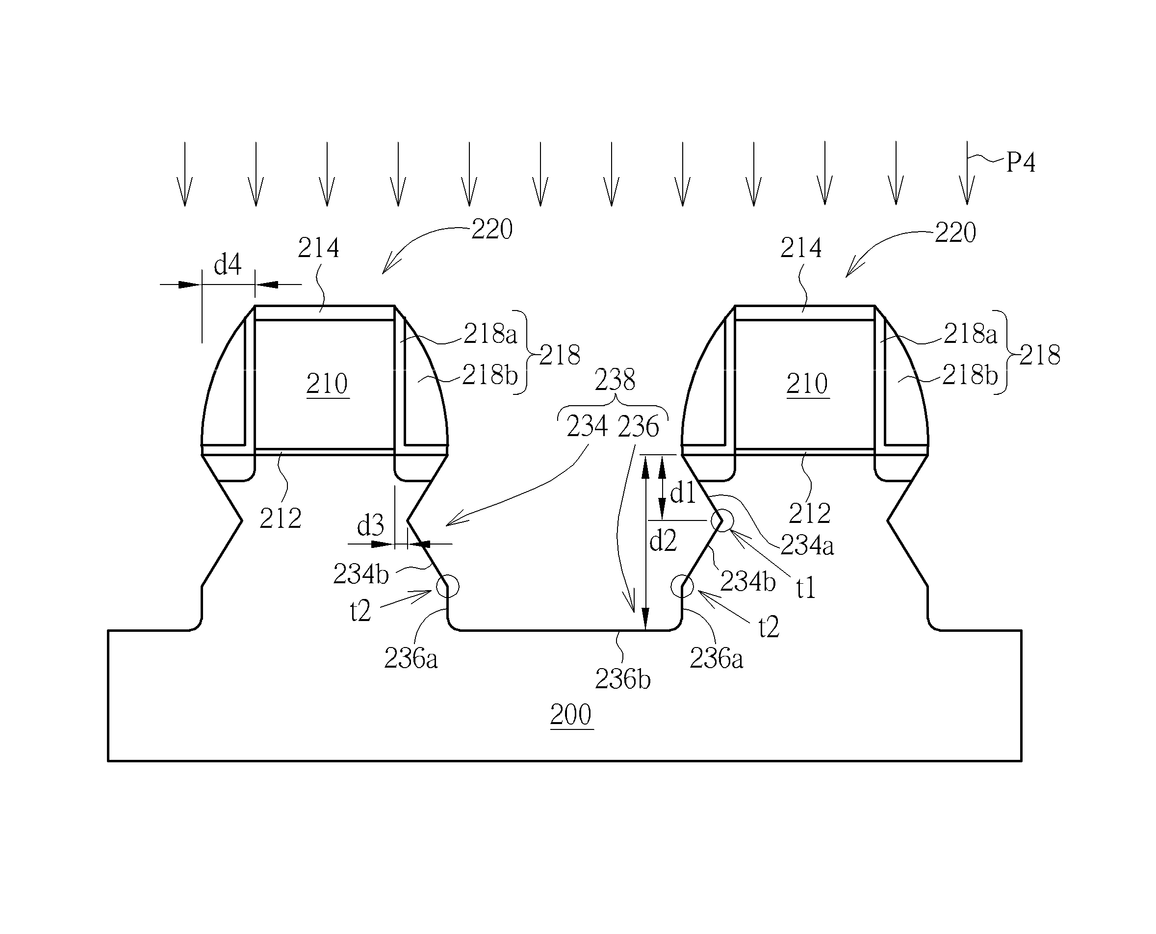
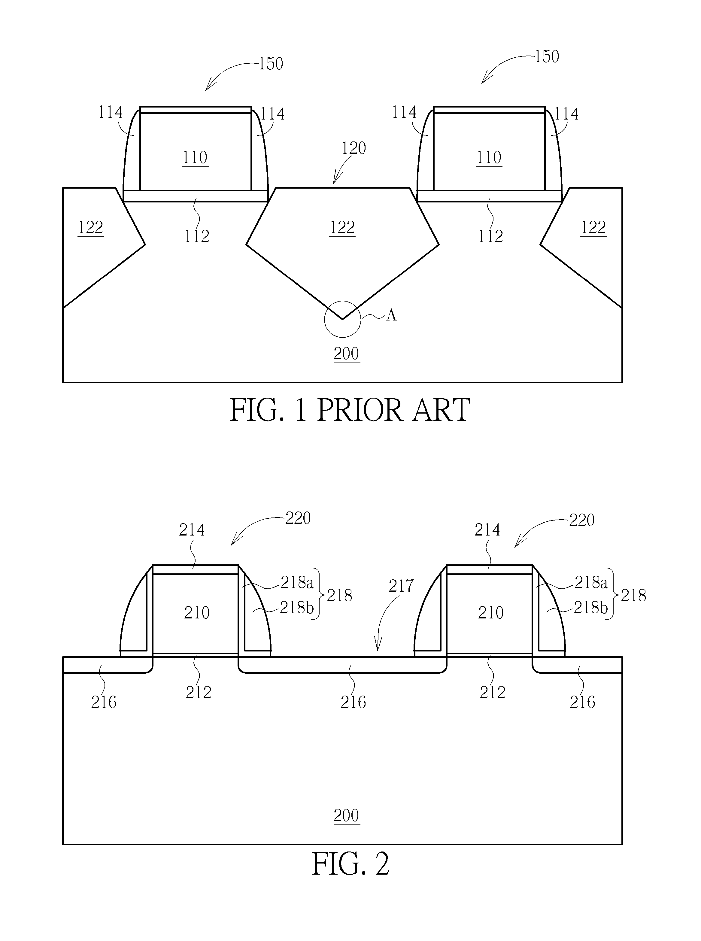
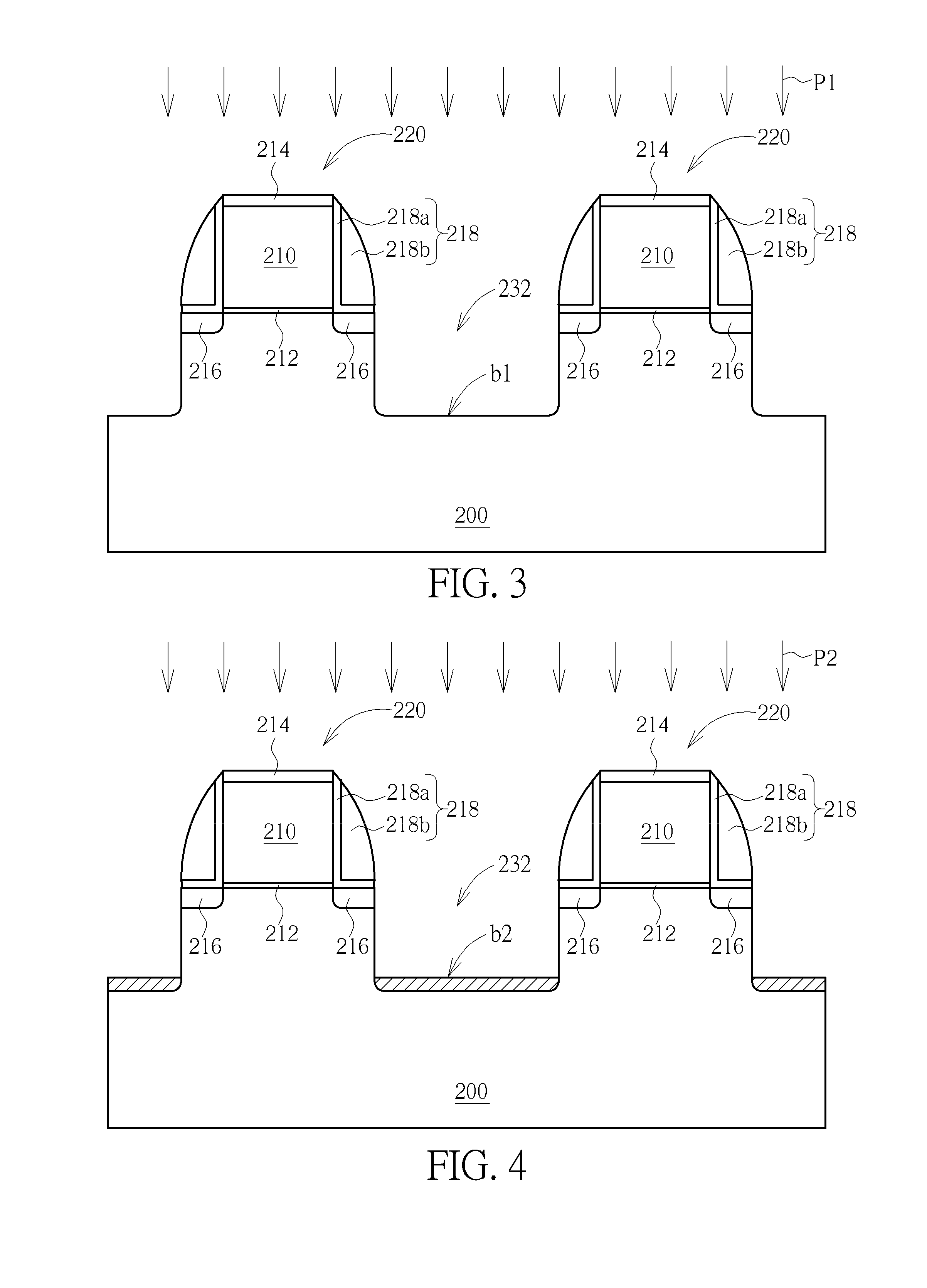
[0019]Please refer to FIGS. 2-7, which are drawings illustrating a manufacturing method for a semiconductor structure provided by a preferred embodiment of the present invention. As shown in FIG. 2, the preferred embodiment first provides a substrate 200. The substrate 200 includes a gate structure 220 formed thereon, and the gate structure 220 includes a gate dielectric layer 212, a gate conductive layer 210, and a cap layer 214 sequentially and upwardly stacked on the substrate 200. It is well-known to those skilled in the art that the cap layer 214 is formed to cover the gate conductive layer 210 to protect the gate conductive layer 210 from damage that may be caused in any process such as photolithograph process, ion implantation, etching process, or any needed cleaning process in the semiconductor fabricating process. LDDs 216 are formed in the substrate 200 at two sides of the gate conductive layer 210 and the gate dielectric layer 212 of the gate structure 220. A spacer 218 i...


PUM


Abstract

The present invention provides a method for forming a semiconductor structure, comprising: firstly, a substrate is provided, next, a first dry etching process is performed, to form a recess in the substrate. Afterwards, an ion implantation process is performed to a bottom surface of the recess, a wet etching process is then performed, to etch partial sidewalls of the recess, so as to form at least two tips on two sides of the recess respectively, and a second dry etching process is performed, to etch partial bottom surface of the recess, wherein after the second dry etching process is performed, a lower portion of the recess has a U-shaped cross section profile.

Description

CROSS REFERENCE TO RELATED APPLICATIONS[0001]This application is a divisional application of U.S. patent application Ser. No. 14 / 714,361 filed May 18, 2015, which is herein incorporated by reference in its entirety.BACKGROUND OF THE INVENTION[0002]1. Field of the Invention[0003]The invention relates to a semiconductor structure and manufacturing method thereof, and more particularly, to a semiconductor structure with a specific shaped epitaxial recess and manufacturing method thereof.[0004]2. Description of the Prior Art[0005]With semiconductor processes entering the era of the deep submicron meter below 65 nanometer (nm), it has been more and more important to increase the metal-oxide semiconductor (MOS) drive current. To improve device performance, a strained-silicon technique such as a selective epitaxial growth (SEG) method is developed to form epitaxial layers serving as the source / drain of the MOS. Because a lattice constant of the epitaxial layer is different from that of sil...

Claims


Application Information

Patent Timeline
Patent Type & Authority Patents(United States)
IPC IPC(8): H01L29/06H01L21/3065H01L21/265H01L21/76H01L29/423H01L21/02H01L21/306
CPCH01L21/02636H01L21/02529H01L21/02532H01L21/26513H01L21/3065H01L21/30604H01L21/76H01L29/0692H01L29/42356H01L21/30608H01L21/26506H01L29/66636H01L29/7834H01L29/7848H01L29/0847H01L29/165H01L21/283
Inventor LIN, YU-YINGCHEN, KUANG-HSIUGUO, TED MING-LANGWANG, YU-REN
Owner UNITED MICROELECTRONICS CORP
Why Eureka
Try Eureka