Light emitting device package

a technology of light-emitting devices and packaging, which is applied in the direction of semiconductor devices, semiconductor/solid-state device details, electrical devices, etc., can solve the problems of heat radiation performance degradation, heat sinks inserted between resin bodies are difficult to have a high process speed, and the optical characteristics of light-emitting devices may be deteriorated

Active Publication Date: 2016-11-29
SUZHOU LEKIN SEMICON CO LTD
View PDF14 Cites 0 Cited by
  • Summary
  • Abstract
  • Description
  • Claims
  • Application Information

AI Technical Summary

Benefits of technology

[0006]In general, after an individual element is manufactured, such a light emitting device is used by packaging the elements. In the light emitting device package, a light emitting chip is mounted on a resin body including a heat sink. The light emitting chip is electrically connected to a lead through a wire. The upper portion of the light emitting chip is filled with a sealing material. A lens is provided on the upper portion. In the light emitting device package having the described structure, since heat generated by operating the light emitting device is slowly transmitted, the light emitting device package has a low heat radiation effect. Therefore, the optical characteristics of the light emitting device may be deteriorated and a package process in which the heat sink is inserted between the resin bodies is difficult to have a high process speed.
[0003]This embodiment relates to a light emitting device package.

Problems solved by technology

Therefore, the optical characteristics of the light emitting device may be deteriorated and a package process in which the heat sink is inserted between the resin bodies is difficult to have a high process speed.
When the light emitting device is mounted on a lead frame without the heat sink, the heat is released through the lead frame, so that heat radiation performance is degraded.
Therefore, a high power light emitting device is difficult to be mounted on the lead frame.
Also, when the resin body which is used in the lead frame for the light emitting device is exposed to the light for a long time, the resin body is discolored or deteriorated, so that the optical characteristics are deteriorated.

Method used


Image

  • Light emitting device package
  • Light emitting device package
  • Light emitting device package

Examples


Embodiment Construction

[0027]A thickness or a size of each layer may be magnified, omitted or schematically shown for the purpose of convenience and clearness of description. The size of each component may not necessarily mean its actual size.

[0028]It should be understood that when an element is referred to as being ‘on’ or “under” another element, it may be directly on / under the element, and / or one or more intervening elements may also be present. When an element is referred to as being ‘on’ or ‘under’, ‘under the element’ as well as ‘on the element’ may be included based on the element.

[0029]An embodiment may be described in detail with reference to the accompanying drawings.

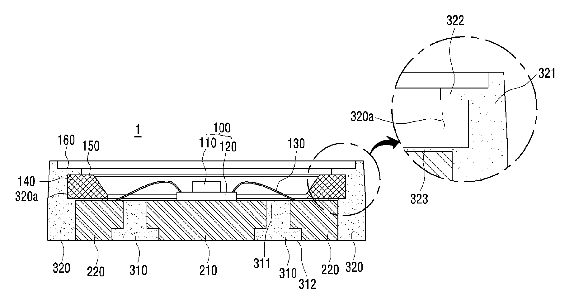
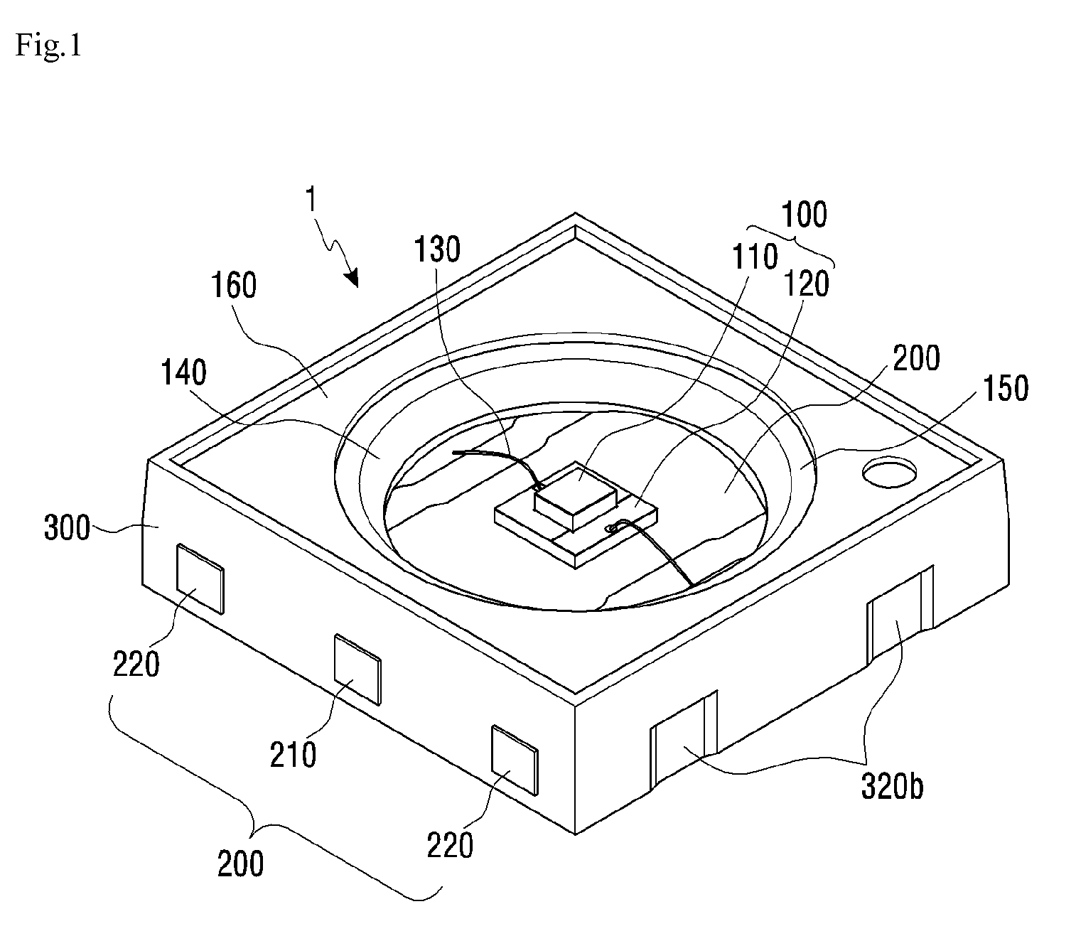
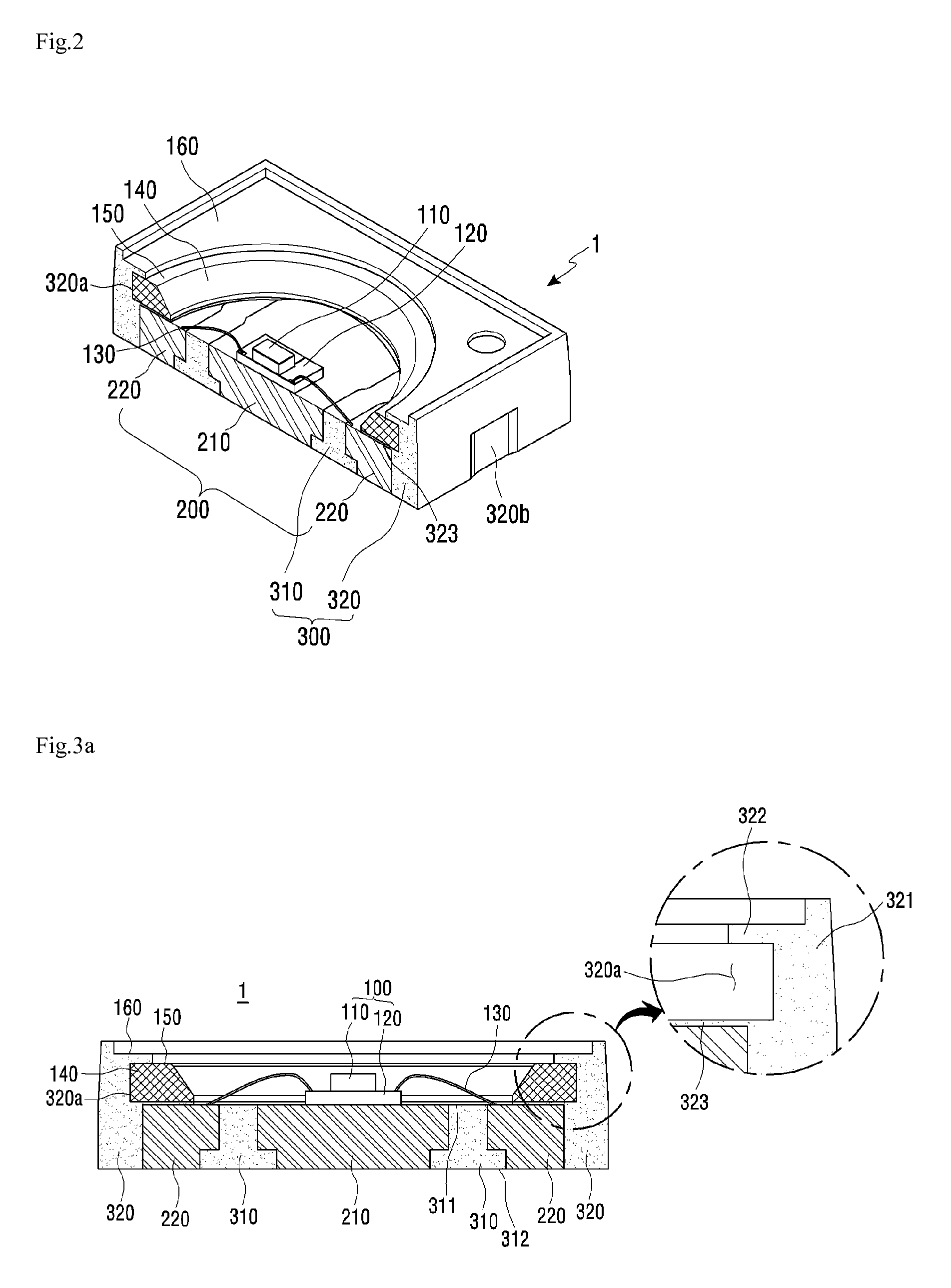
[0030]FIG. 1 is a perspective view of a light emitting device package according to an embodiment. FIG. 2 is a sectional perspective view of the light emitting device package according to the embodiment shown in FIG. 1. FIG. 3a is a cross sectional view of the light emitting device package according to the embodiment shown in FIG. 2....


PUM


Abstract

A light emitting device package may be provided that includes: a lead frame which includes a first frame and a second frame disposed on both sides of the first frame respectively; a light emitting device which is disposed on the first frame and is electrically connected to the second frame; and a resin body which includes a first resin body which is disposed between the first frame and the second frame, and a second resin body which covers an outer surface of the lead frame. An end of the first frame and an end of the second frame are disposed on an outer surface of the second resin body.

Description

CROSS-REFERENCE TO RELATED APPLICATION[0001]The present application claims priority under 35 U.S.C. §119(a) of Korean Patent Application Nos. 10-2014-0084907 and 10-2014-0084908 filed Jul. 8, 2014, the subject matters of which are incorporated herein by reference.BACKGROUND[0002]Field[0003]This embodiment relates to a light emitting device package.[0004]Description of Related Art[0005]A light emitting diode (LED) is a light source with high efficiency and environmental friendliness and becomes popular in a variety of fields. The LED is being used in various fields, for example, a display, optical communication, an automobile and general lighting. Particularly, demand for a white light emitting diode creating white light is gradually increasing.[0006]In general, after an individual element is manufactured, such a light emitting device is used by packaging the elements. In the light emitting device package, a light emitting chip is mounted on a resin body including a heat sink. The li...

Claims


Application Information

Patent Timeline
Patent Type & Authority Patents(United States)
IPC IPC(8): H01L33/56H01L33/62H01L33/48H01L23/00H01L33/54H01L33/60H01L33/64
CPCH01L33/56H01L24/97H01L33/486H01L33/54H01L33/62H01L33/647H01L33/60H01L33/642H01L2224/48091H01L2224/48247H01L2924/00014H01L33/48H01L2933/0066H01L2933/0075H01L2933/005
Inventor OZEKI, SATOSHITANDA, YUICHIRO
Owner SUZHOU LEKIN SEMICON CO LTD
Why Eureka
Try Eureka