Unlock instant, AI-driven research and patent intelligence for your innovation.

Solid state photomultiplier

a photomultiplier and solid state technology, applied in the field of solid state photomultipliers, can solve the problems of signal integrity degradation, additional noise, and detector crosstalk, and achieve the effect of improving the solid state photomultiplier

Active Publication Date: 2017-02-14
GENERAL ELECTRIC CO
View PDF14 Cites 12 Cited by
  • Summary
  • Abstract
  • Description
  • Claims
  • Application Information

AI Technical Summary

Benefits of technology

This approach effectively reduces noise and crosstalk, enhancing signal integrity by allowing AC coupling of high voltage signals to low voltage components, improving the performance of solid state photomultipliers in imaging systems like PET and SPECT.

Problems solved by technology

However, due to stray or parasitic capacitance along the signal path, the signal may be degraded, thereby causing the detector to suffer from crosstalk, signal integrity degradation and additional noise.
Moreover, such configurations may still suffer crosstalk between the high voltage components (SPAD) and low voltage components (readout electronics).

Method used


Image

  • Solid state photomultiplier
  • Solid state photomultiplier
  • Solid state photomultiplier

Examples


Embodiment Construction

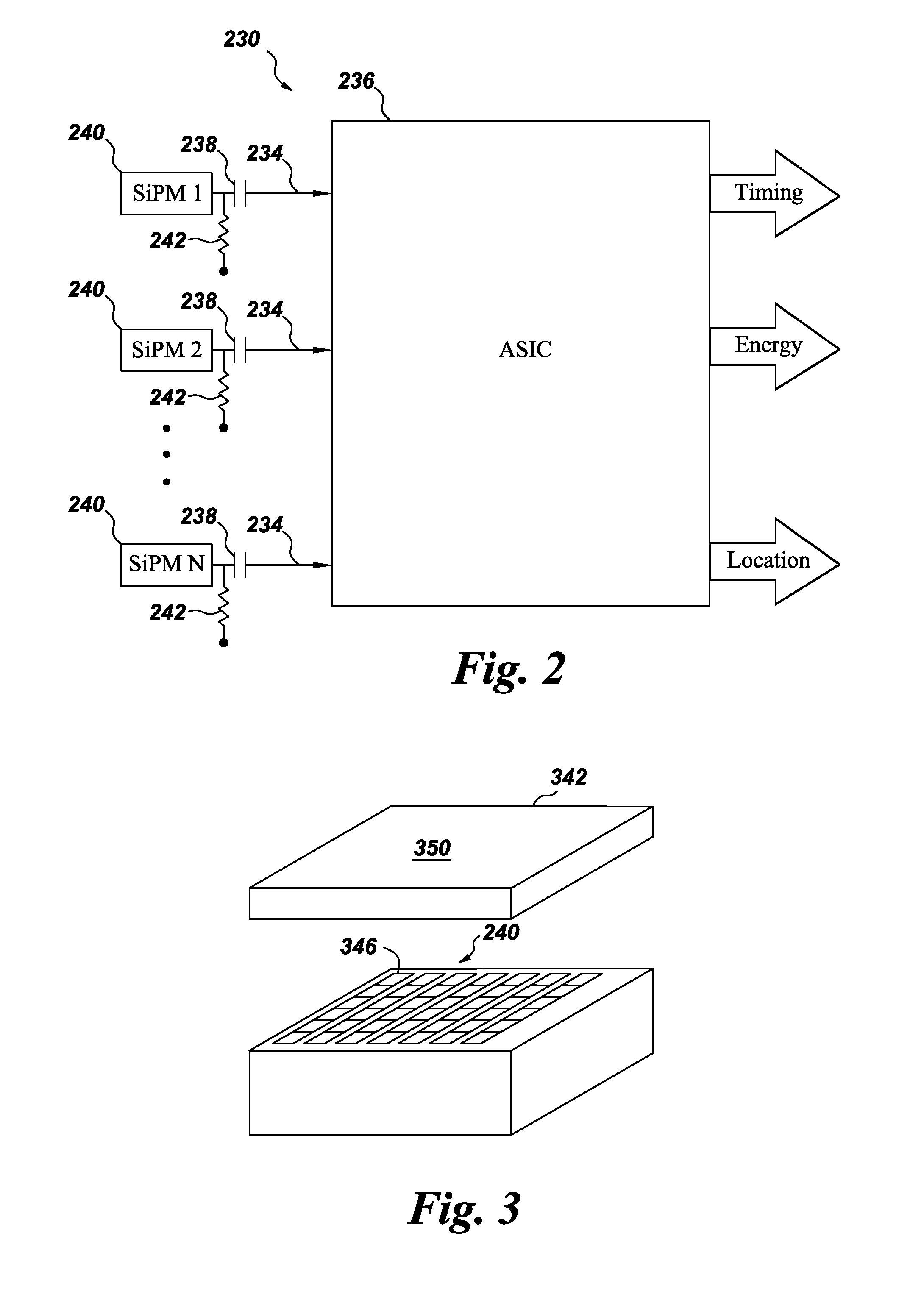
[0022]Embodiments of a solid state photomultiplier are disclosed herein. In at least some embodiments, the inventive solid state photomultiplier advantageously utilizes a low voltage well that isolates low voltage readout electronics (e.g. buffers, comparators, or the like.) from the high voltage components (e.g. photodiodes such as a single-photon avalanche diode (SPAD), or the like) to form a capacitor that facilitates an AC coupling of the signal generated by the high voltage components to the readout electronics. Furthermore, this mechanism may further advantageously be extended to allow the fabrication of on-chip capacitors for AC coupling the high voltage signal to off-chip readout electronics.

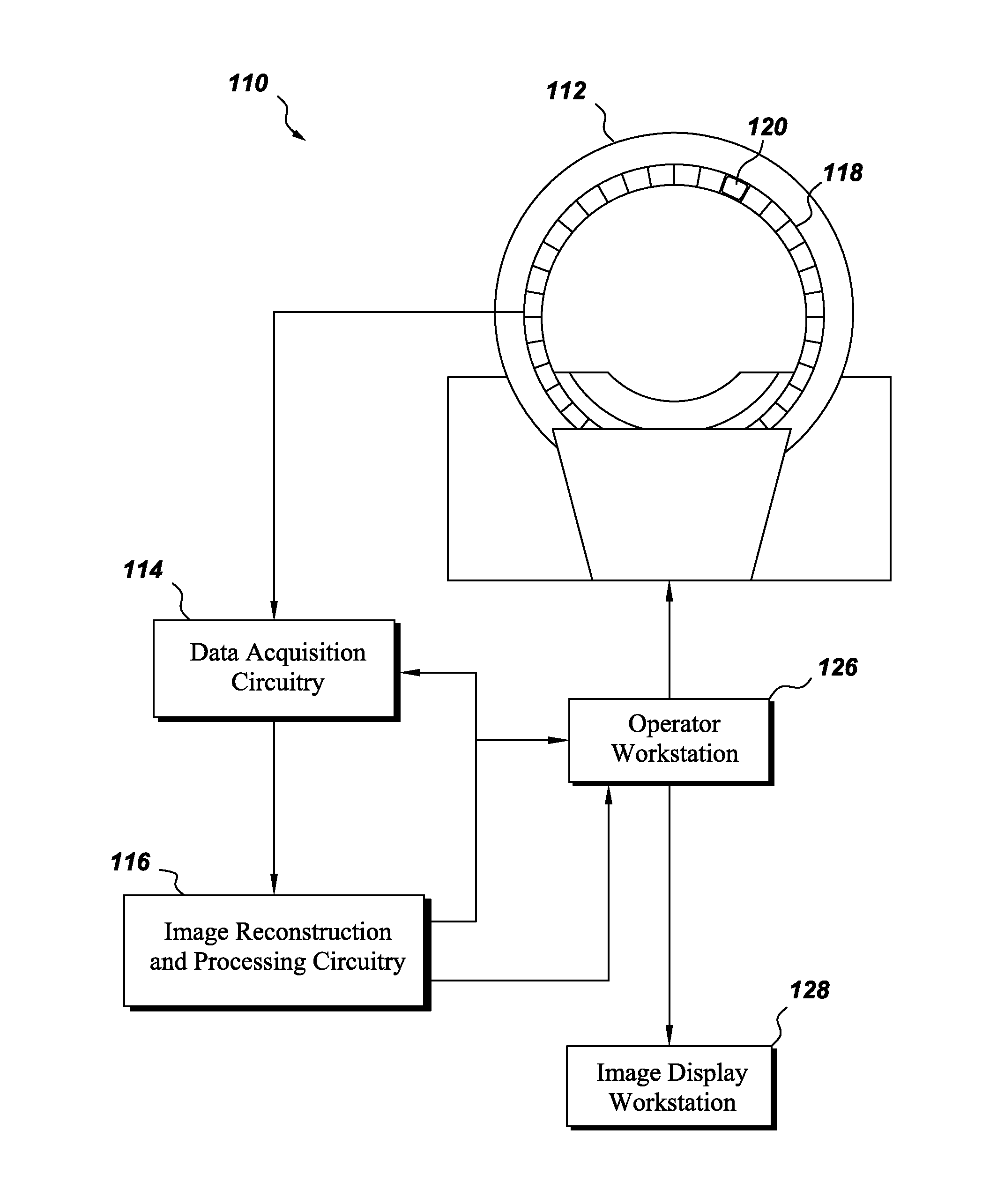
[0023]Embodiments discussed herein relate to a detector in a nuclear imaging system, such as a positron emission tomography (PET) or single photon emission computed tomography (SPECT) imaging system or in a combined or hybrid imaging system including such PET or SPECT imaging functionali...


PUM


Abstract

Embodiments of a solid state photomultiplier are provided herein. In some embodiments, a photosensor may include a sensing element; and readout electronics, wherein the sensing element is AC coupled to the readout electronics. In some embodiments, a solid state photomultipler may include a microcell having; a sensing element; and readout electronics, wherein the sensing element is AC coupled to the readout electronics.

Description

CROSS REFERENCE TO RELATED APPLICATION[0001]This patent application claims the benefit of priority, under 35 U.S.C. §119, of U.S. Provisional Patent Application Ser. No. 62 / 053487, filed Sep. 22, 2014, titled “SOLID STATE PHOTOMULTIPLIER” the entire disclosure of which is incorporated herein by reference.BACKGROUND[0002]The subject matter disclosed herein generally relates to detectors for use in imaging systems, such as X-ray, nuclear medicine imaging systems, combinations thereof, or the like.[0003]Conventional imagining technologies generally include one or more detectors configured to convert incident radiation to useful electrical signals that can be used in image formation. Such detectors may employ solid state photomultipliers (e.g., silicon photomultipliers (SiPM)), which may be useful for detecting optical signals generated in a scintillator in response to the incident radiation. Typical mechanisms utilized to read out analog SSPM pixels may include either AC or DC coupling...

Claims


Application Information

Patent Timeline
Patent Type & Authority Patents(United States)
IPC IPC(8): G01T1/24H04N5/32H01L31/107
CPCG01T1/248G01T1/247G01T1/249H01L31/107H04N5/32H01L27/14603H01L27/14609H01L27/14663
Inventor GUO, JIANJUNDOLINSKY, SERGEI IVANOVICHMCDANIEL, DAVID LEOSHORT, JONATHAN DAVID
Owner GENERAL ELECTRIC CO