Metal base substrate, power module, and method for manufacturing metal base substrate

a technology of metal base substrate and power module, which is applied in the direction of printed circuit manufacturing, printed circuit aspects, and metal adhesion improvement of insulating substrates, can solve the problems insulating layer fails to secure a thickness, and fails to maintain a withstand voltage, so as to achieve the effect of reducing withstand voltage and facilitating manufacturing

Active Publication Date: 2017-02-21
MITSUBISHI ELECTRIC CORP
View PDF9 Cites 2 Cited by
  • Summary
  • Abstract
  • Description
  • Claims
  • Application Information

AI Technical Summary

Benefits of technology

[0007]The present invention has been made in view of the above-mentioned problems, and an object thereof is to provide a metal base substrate that can suppress a decrease in withstand voltage and can easily be manufactured, a power module, and a method for manufacturing the metal base substrate.
[0009]In the present invention, the metal base substrate includes the substrate made of copper, the first metal layer that is formed on the substrate and is made of the metal different from the copper, the insulating resin sheet that is formed by bonding the sheet made of the insulating resin onto the first metal layer, and the circuit pattern formed on the insulating resin sheet. Thus, the metal base substrate can suppress a decrease in withstand voltage and can easily be manufactured.

Problems solved by technology

In Japanese Patent Application Laid-Open No. 6-350213 (1994), the liquid epoxy resin is applied on the copper plate to form the insulating layer, so that the insulating layer fails to secure a thickness thereof and fails to maintain a withstand voltage.
Moreover, a pinhole is formed in the insulating layer formed by the application of the liquid epoxy resin, whereby the withstand voltage may possibly decrease.
Furthermore, the problem arises that a manufacturing process in manufacturing the configuration mentioned above becomes complicated.

Method used


Image

  • Metal base substrate, power module, and method for manufacturing metal base substrate
  • Metal base substrate, power module, and method for manufacturing metal base substrate
  • Metal base substrate, power module, and method for manufacturing metal base substrate

Examples


first preferred embodiment

[0016]First, a configuration of a metal base substrate according to a first preferred embodiment of the present invention will be described.

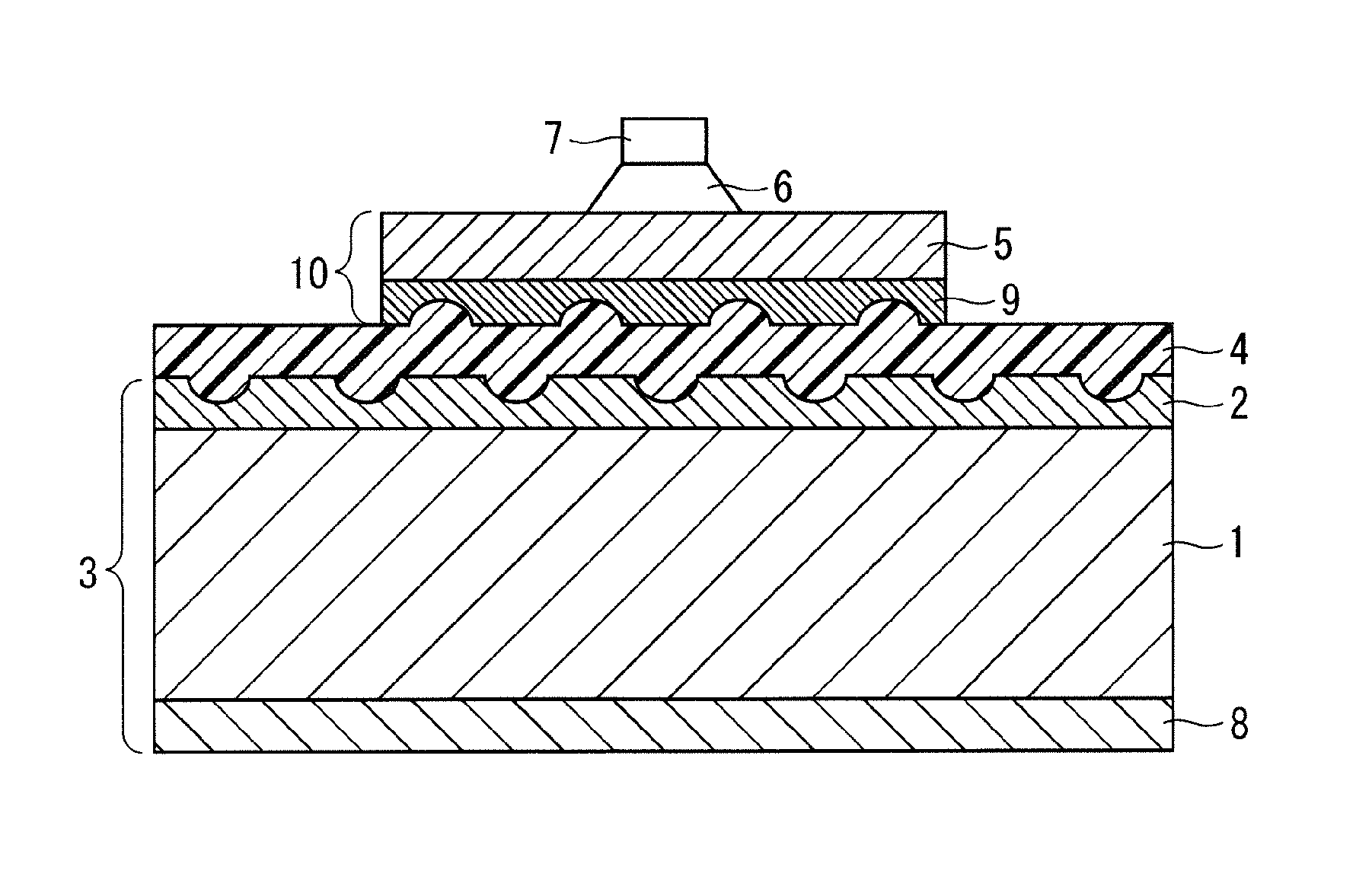
[0017]FIG. 1 is a diagram showing an example of the configuration of the metal base substrate according to the first preferred embodiment.

[0018]As shown in FIG. 1, a metal layer 2 (first metal layer) is bonded onto a copper plate 1 (substrate made of copper), and the copper plate 1 and the metal layer 2 form a cladding base plate 3. Here, the metal layer 2 may be made of, for example, aluminum or an aluminum alloy that is a kind of metal different from copper and a metal having good adhesion properties to an insulating resin sheet 4 described later.

[0019]The insulating resin sheet 4 that is formed by bonding a sheet made of an insulating resin onto the metal layer 2. The insulating resin sheet 4 is made of an epoxy resin, for example. Here, the insulating resin sheet 4 may be individually bonded to the metal layer 2 and may also be bonded to the...

second preferred embodiment

[0042]FIG. 5 is a diagram showing an example of a configuration of a power module according to a second preferred embodiment of the present invention.

[0043]As shown in FIG. 5, the power module includes the metal base substrate according to the first preferred embodiment, a case 15 having the metal base substrate as a lower surface, a power terminal 11 and a signal terminal 12 having one ends electrically connected to the semiconductor chip 7 mounted on the circuit pattern 5 of the metal base substrate, and a resin (resins 17 and 18) that fills the case 15 so as to expose at least the other ends of the power terminal 11 and the signal terminal 12.

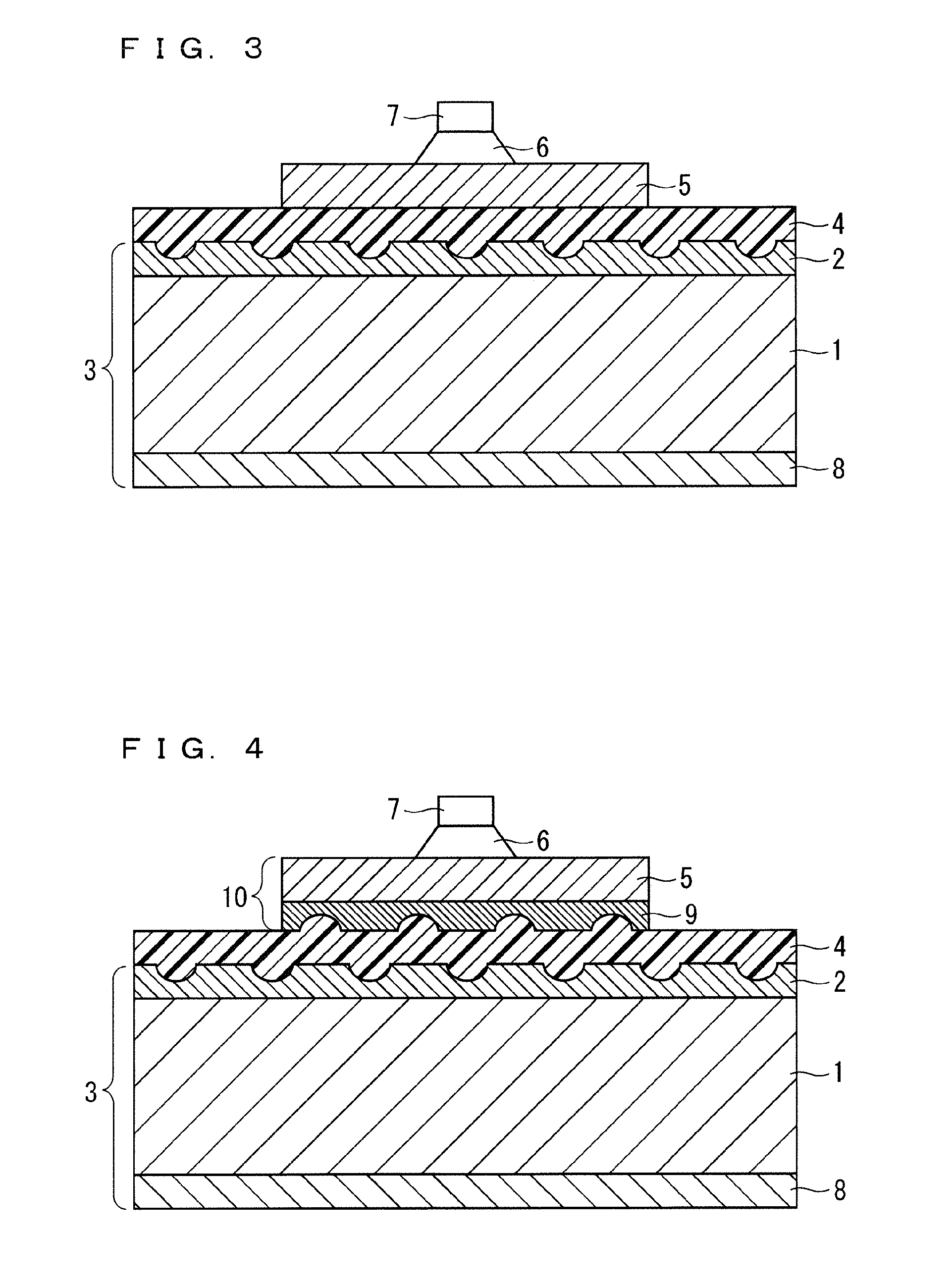
[0044]In addition, the metal base substrate shown in FIG. 5 shows the case where the metal layer 8 as shown in FIG. 3 is formed on the back surface of the copper plate 1 in the metal base substrate shown in FIG. 1 as an example, but it suffices that the metal base substrate shown in FIG. 5 is as long as the metal base substrate according to ...

first modification

[0049]FIG. 6 is a diagram showing the other example of the configuration of the power module.

[0050]As shown in FIG. 6, the power module according to the first preferred modification is characterized in that a resin 19 is a solid resin. The other configuration is similar to that in FIG. 5, so that descriptions will be omitted here.

[0051]The resin 19 is the solid resin and may be a solid epoxy resin, for example. A method for filling the case 15 with the resin 19 may be potting, for example.

[0052]As described above, the metal base substrate according to the first preferred embodiment can be applied to the power module in which a change in shape occurs due to a change in temperature. Particularly in a case where the resin being the filling material is solid, the resin can fix the structural components that are objects to be sealed, but stress is caused by each of different thermal expansion coefficients of a circuit pattern, an insulating layer, and a cladding base plate, resulting in ...


PUM

PropertyMeasurementUnit
insulatingaaaaaaaaaa
heat dissipation propertiesaaaaaaaaaa
adhesion propertiesaaaaaaaaaa

Abstract

A metal base substrate of the present invention includes a copper plate made of copper, a metal layer that is formed on the copper plate and is made of a metal different from the copper, an insulating resin sheet that is formed by bonding a sheet made of an insulating resin onto the metal layer, and a circuit pattern formed on the insulating resin sheet.

Description

BACKGROUND OF THE INVENTION[0001]Field of the Invention[0002]The present invention relates to a metal base substrate for a semiconductor device, a power module including the metal base substrate, and a method for manufacturing the metal base substrate.[0003]Description of the Background Art[0004]In the field of power electronics or the like, a metal substrate having a semiconductor chip mounted thereon is conventionally used to secure heat dissipation properties for heat generated in the semiconductor chip while being electrically insulated from the semiconductor chip, for example.[0005]For example, in a case where a copper plate is used as a metal substrate, aluminum (or aluminum alloy) is rolled on one side (surface on the side on which an insulating layer is formed) of the copper plate to form a cladding base plate, in order to improve adhesion properties (adhesion strength) between the copper plate and the insulating layer formed on the copper plate. A liquid epoxy resin is appl...

Claims


Application Information

Patent Timeline
Patent Type & Authority Patents(United States)
IPC IPC(8): H01L21/00H01L23/48H05K1/05H01L21/48H05K3/44H01L23/043H05K3/38H01L23/24H01L23/053H05K1/09H01L23/373H01L23/14H05K1/03H01L23/495H01L23/31H01L23/29H01L23/00H01L23/498
CPCH01L23/043H01L23/053H01L23/14H01L23/24H01L23/296H01L23/3107H01L23/3735H01L23/48H01L23/49534H01L23/49541H01L23/49582H01L23/49586H01L24/40H01L24/49H05K1/0326H05K1/056H05K1/09H05K3/38H05K3/44H01L21/4828H01L21/4842H01L23/3736H01L23/49861H01L24/32H01L24/48H01L2224/291H01L2224/32225H01L2224/40095H01L2224/40225H01L2224/48091H01L2224/48137H01L2224/48177H01L2224/48227H01L2224/73265H01L2924/0665H01L2924/1033H01L2924/10253H01L2924/10272H01L2924/17724H01L2924/17747H01L2924/181H01L2924/19107H05K3/381H05K3/383H05K2201/066H05K2203/06H01L2924/00014H01L2924/00012H01L2924/014H01L2924/00H05K3/388H01L2224/83801H01L2224/84801H01L2224/84205H01L24/84H01L2224/73221H01L2224/45099H01L2224/45015H01L2924/207H01L2224/37099
Inventor ONO, MARIKOGOTO, AKIRAYONEYAMA, REIOTSUKI, TAKAMI
Owner MITSUBISHI ELECTRIC CORP
Why Eureka
Try Eureka