Method of forming semiconductor device

Active Publication Date: 2017-03-07
UNITED MICROELECTRONICS CORP
View PDF15 Cites 4 Cited by
  • Summary
  • Abstract
  • Description
  • Claims
  • Application Information

AI Technical Summary

Benefits of technology

[0009]The method set for the in the present invention is characterized that there is no oxygen treatment performed after exposing the second trench and before forming the third sacrificial layer. Thus, the

Problems solved by technology

With a trend toward scaling down the size of semiconductor devices, the conventional poly-silicon gate has faced problems such as inferior performance due to boron penetration and unavoidable depletion effect which increases equivalent thickness of the gate dielectric layer, reduces gate capacitance, and worsens a driving force of the devices.
However, because of the

Method used


Image

  • Method of forming semiconductor device
  • Method of forming semiconductor device
  • Method of forming semiconductor device

Examples


Example

[0020]To provide a better understanding of the presented invention, preferred embodiments will be made in detail. The preferred embodiments of the present invention are illustrated in the accompanying drawings with numbered elements.

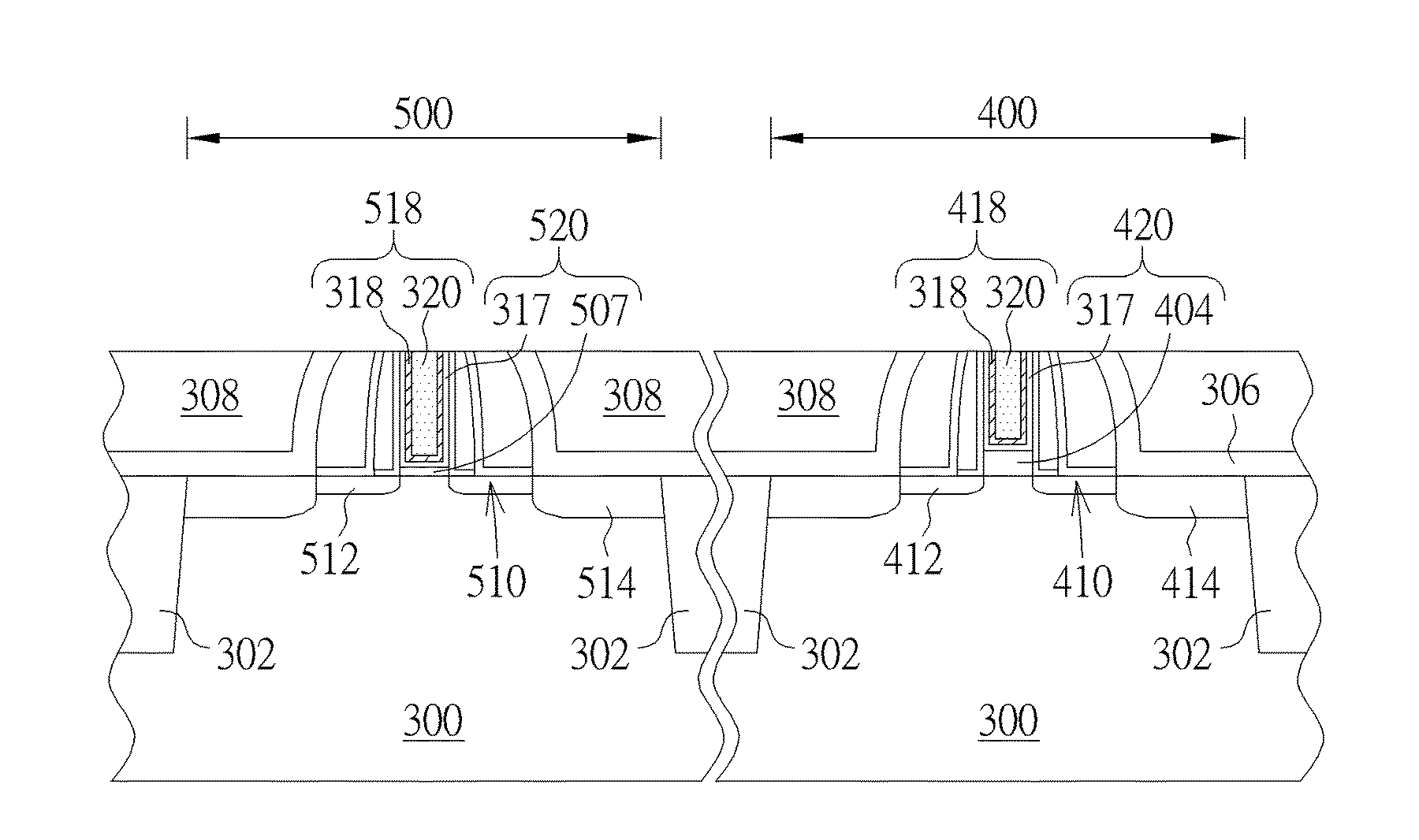
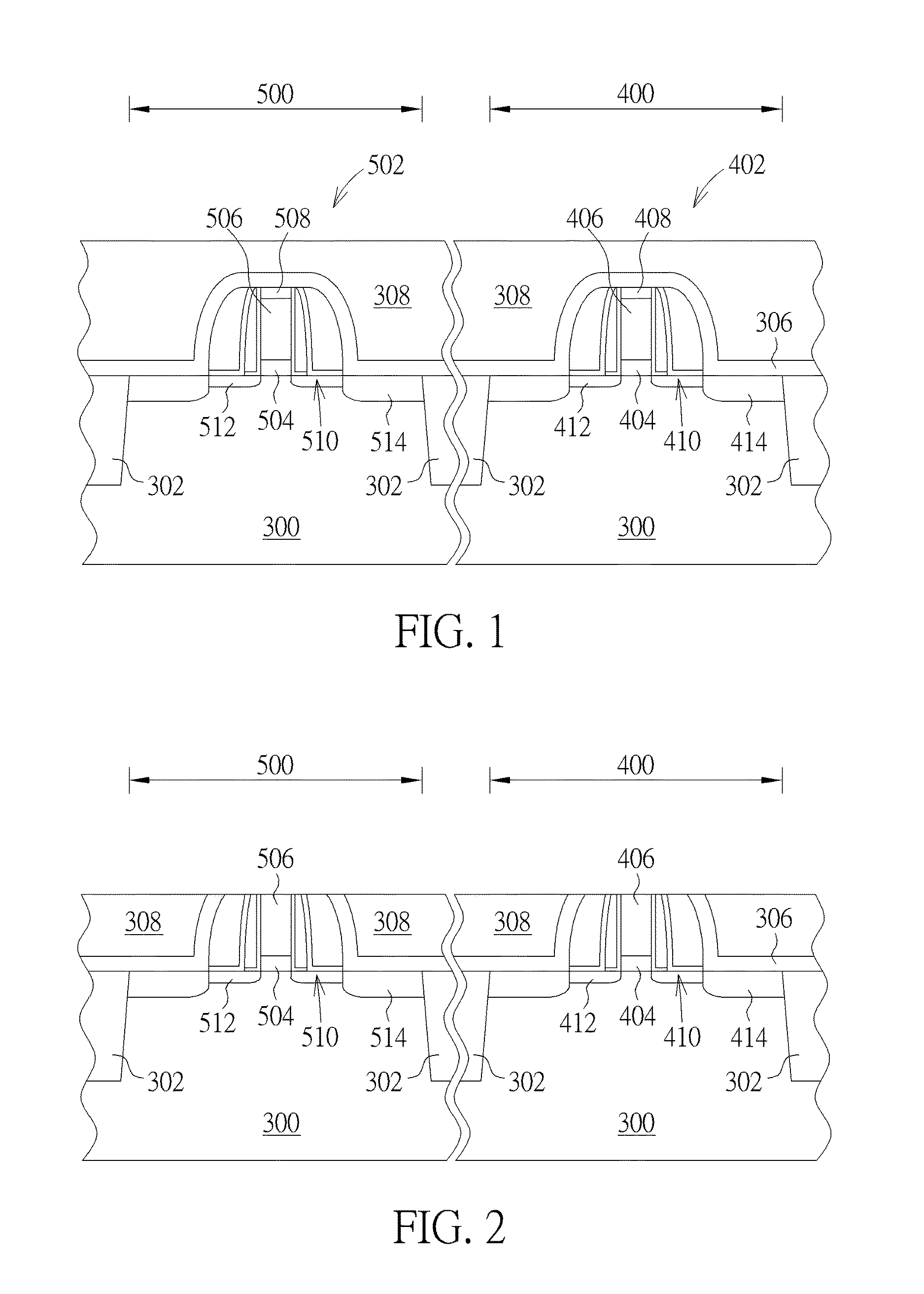
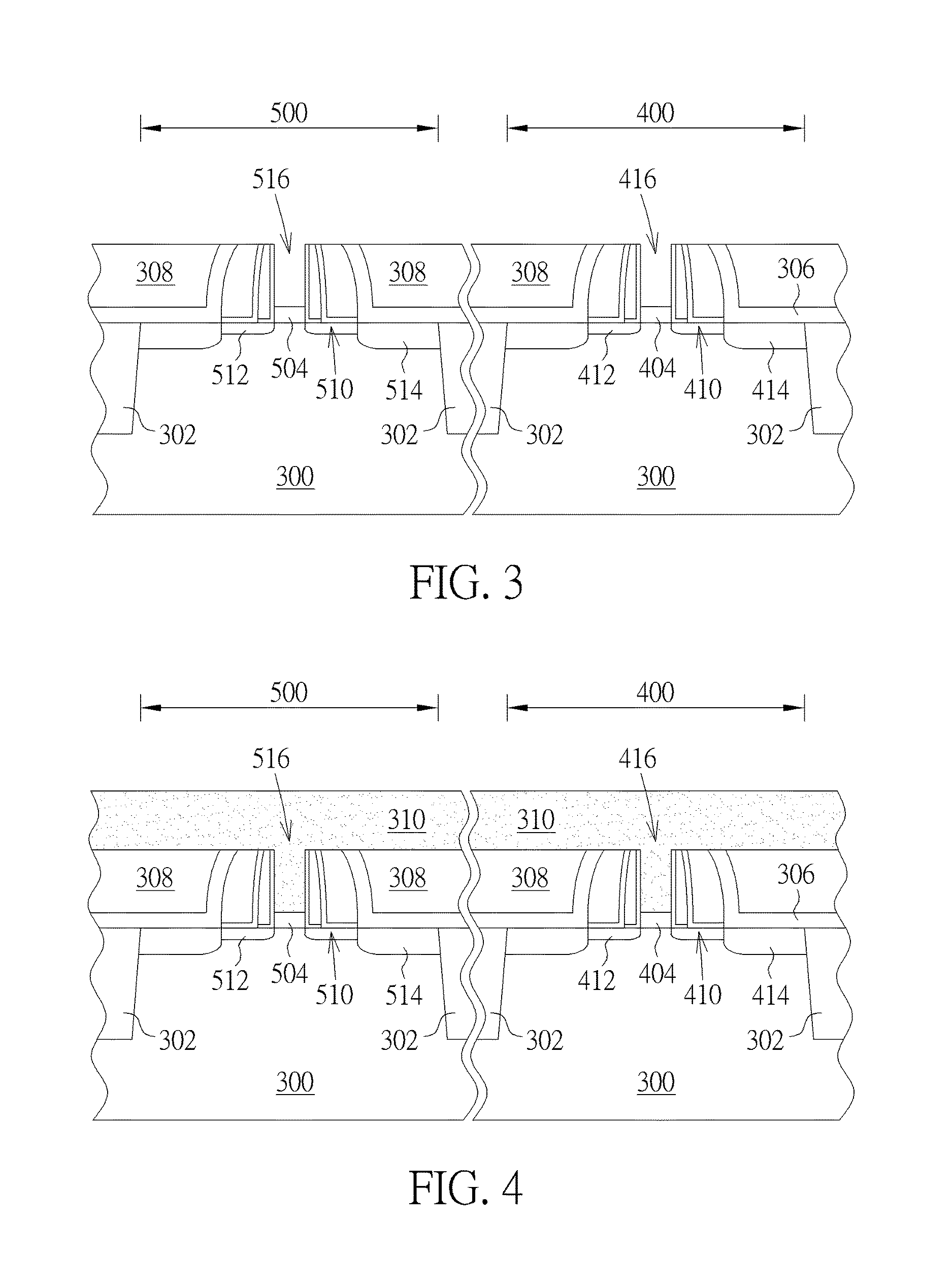
[0021]Please refer to FIG. 1 to FIG. 9, showing schematic diagrams of the method for forming a semiconductor device according to one embodiment of the present invention. Please refer to FIG. 1, a substrate 300 is provided to serve as a base for forming devices, components, or circuits. The substrate 300 is preferably composed of a silicon containing material. Silicon containing materials include, but are not limited to, Si, single crystal Si, polycrystalline Si, SiGe, single crystal silicon germanium, polycrystalline silicon germanium, or silicon doped with carbon, amorphous Si and combinations and multi-layered materials thereof. The semiconductor substrate 300 may also be composed of other semiconductor materials, such as germanium, and compound semico...


PUM


Abstract

A method for forming a semiconductor device is provided. First, a dielectric layer is provided on a substrate, wherein a first recess and a second recess are formed in the dielectric layer. After a mask layer is filled into the first recess and the second recess, the mask layer in the second recess is removed away, thereby forming a patterned mask layer. Subsequently, a nitride treatment is performed to remove unwanted residue of the mask layer in the second recess.

Description

BACKGROUND OF THE INVENTION[0001]1. Field of the Invention[0002]The present invention relates to a method of fabricating a semiconductor device, and more particularly, to a method of simultaneously forming a high-voltage device and a low-voltage device.[0003]2. Description of the Prior Art[0004]With a trend toward scaling down the size of semiconductor devices, the conventional poly-silicon gate has faced problems such as inferior performance due to boron penetration and unavoidable depletion effect which increases equivalent thickness of the gate dielectric layer, reduces gate capacitance, and worsens a driving force of the devices. Therefore, work function metals that are suitable for use as the high-k gate dielectric layer are used to replace the conventional poly-silicon gate to be the control electrode.[0005]The conventional metal gate methods are categorized into gate first processes and gate last processes. In a conventional gate first process, the annealing process for formi...

Claims


Application Information

Patent Timeline
IPC IPC(8): H01L21/82H01L29/66H01L21/8234
CPCH01L21/823462H01L29/66545H01L29/4966H01L29/7833
Inventor TSAI, FU-YULIU, WEI-HSINHUANG, HAN-SHENG
Owner UNITED MICROELECTRONICS CORP
Why Eureka
Try Eureka