Method for manufacturing semiconductor device

a semiconductor and manufacturing technology, applied in the direction of semiconductor devices, basic electric elements, electrical equipment, etc., can solve the problems of increased defect density in the channel region of the substrate, deformation of uniform uniformity, and degraded electrical performance and so as to ensure the reliability of the device, reduce the cost, and simplify the process

Active Publication Date: 2016-12-27
INST OF MICROELECTRONICS CHINESE ACAD OF SCI
View PDF9 Cites 0 Cited by
  • Summary
  • Abstract
  • Description
  • Claims
  • Application Information

AI Technical Summary

Benefits of technology

[0007]As stated above, the present invention aims to provide a method for manufacturing a semiconductor device that can protect the substrate from overetching in the gate last process with high efficiency and low cost.
[0017]In accordance with the method for manufacturing a semiconductor device of the present invention, the dummy gate made of carbon-based materials is used to substitute the dummy gate made of silicon-based materials, then no oxide liner and / or etch blocking layer needs be added while the dummy gate is removed by etching in the gate last process, thus the reliability of device is ensured while the process is simplified and the cost is reduced.

Problems solved by technology

Since the dummy gate is made of a material similar to that of the substrate, both of which are made of silicon-based materials, the substrate will be inevitably overetched in the process of etching the dummy gate, resulting in an increase in the defect density in the surface of the channel region of the substrate, and thus the electrical performance and reliability of the device are degraded.
However, the oxide liner and / or the etch blocking layer has an ultra-thin thickness, so it is hard to be formed uniformly.
Besides, formation of such an ultra-thin oxide liner and / or etch blocking layer involves complicated processes and expensive materials, hence it is hardly applicable to mass manufacture of the device, and it is difficult to improve efficiency and reduce cost effectively.
In summary, in the prior art it is difficult to protect the substrate from overetching in the gate last process with high efficiency and low cost.

Method used


Image

  • Method for manufacturing semiconductor device
  • Method for manufacturing semiconductor device
  • Method for manufacturing semiconductor device

Examples


Embodiment Construction

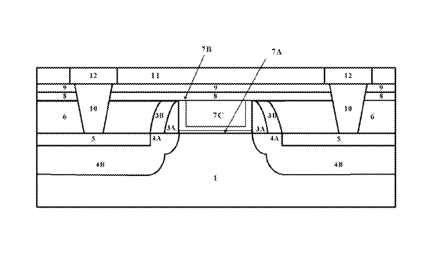
[0021]The features and the technical effects of the technical solution of the present application will be described in detail in combination with the illustrative embodiments with reference to the drawings, and disclosed herein is a method for manufacturing a semiconductor device that is capable of simplifying the removal of a dummy gate effectively. It should be pointed out that like reference signs indicate like structures, the terms such as “first”, “second”, “on”, “below” used in the present invention may be used to modify various device structures or manufacturing processes. Except for specific explanations, these modifications do not imply the spatial, sequential or hierarchical relationships of the structures of the modified device or the manufacturing processes.

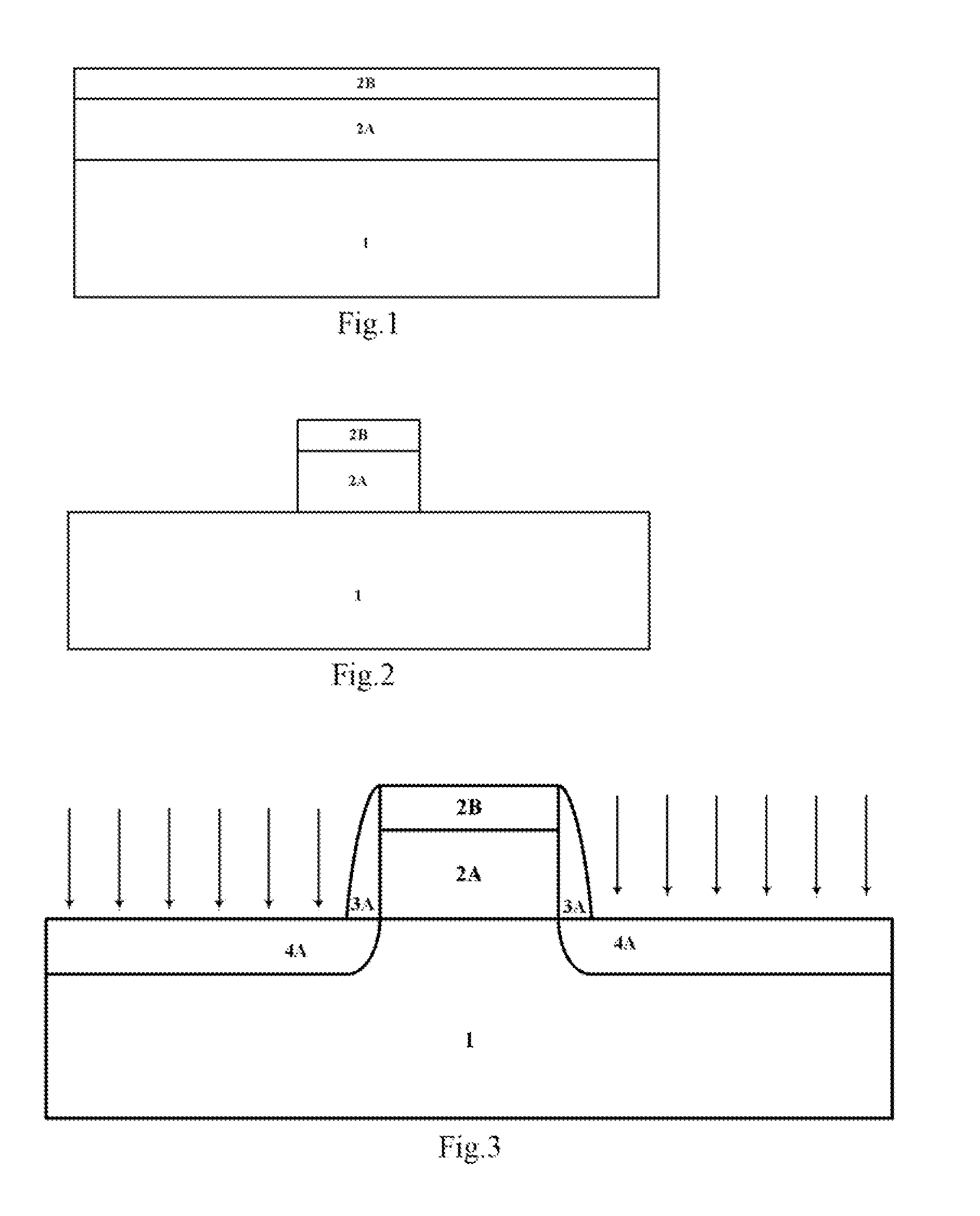
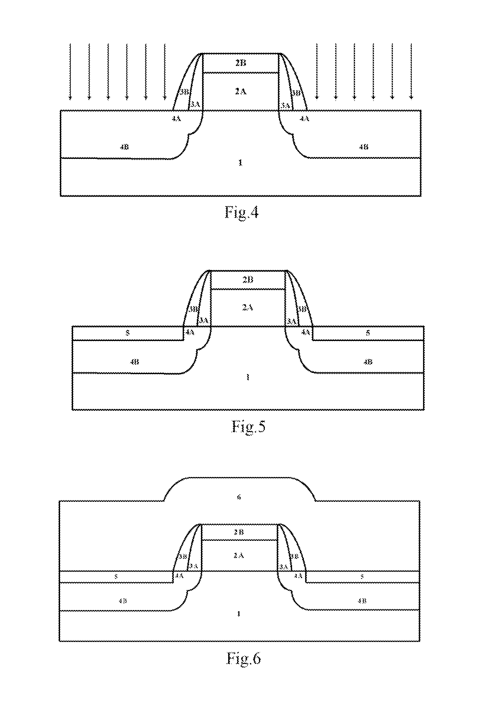
[0022]FIGS. 1 to 14 are diagrammatic cross-sections of the steps of the method for manufacturing a semiconductor device in accordance with the present invention.

[0023]Referring to FIG. 15 and FIGS. 1 and 2, a dummy ga...


PUM


Abstract

The present invention discloses a method for manufacturing a semiconductor device, comprising the steps of: forming a dummy gate stack structure on a substrate, wherein the dummy gate stack structure contains carbon-based materials; forming source / drain region in the substrate on both sides of the dummy gate stack structure; performing etching to remove the dummy gate stack structure until the substrate is exposed, resulting in a gate trench; and forming a gate stack structure in the gate trench. In accordance with the method for manufacturing a semiconductor device of the present invention, the dummy gate made of carbon-based materials is used to substitute the dummy gate made of silicon-based materials, then no oxide liner and / or etch blocking layer needs be added while the dummy gate is removed by etching in the gate last process, thus the reliability of device is ensured while the process is simplified and the cost is reduced.

Description

CROSS REFERENCE[0001]This application is a National Phase application of, and claims priority to, PCT Application No. PCT / CN2012 / 000912, filed on Jul. 3, 2012, entitled ‘METHOD FOR MANUFACTURING A SEMICONDUCTOR DEVICE’, which claimed priority to Chinese Application No. CN 201210140207.X, filed on May 8, 2012. Both the PCT Application and Chinese Application are incorporated herein by reference in their entireties.FIELD OF THE INVENTION[0002]The present invention relates to a method for manufacturing a semiconductor device, in particular relates to a method for manufacturing a semiconductor device that is applied to a gate last process.BACKGROUND OF THE INVENTION[0003]The device size is required to be scaled down as the IC integration level constantly increases. In order to solve a series of problems caused by scaling down of the MOS device, the traditional SiO2 / polysilicon gate structure is generally substituted by the high-K / metal gate stack structure. Currently, the process for ma...

Claims


Application Information

Patent Timeline
Patent Type & Authority Patents(United States)
IPC IPC(8): H01L29/66H01L29/78H01L21/28H01L29/49H01L29/51
CPCH01L29/66545H01L21/28008H01L29/7833H01L29/4966H01L29/517
Inventor YIN, HAIZHOUZHANG, KEKE
Owner INST OF MICROELECTRONICS CHINESE ACAD OF SCI
Why Eureka
Try Eureka