Supercharge Your Innovation With Domain-Expert AI Agents!

Arrays of integrated analytical devices

a technology of integrated analytical devices and arrays, applied in the field of analytical systems, can solve the problems of reducing the signal to noise ratio resulting from either or both of lower signals, increasing the difficulty of multiplexing and increasing the difficulty of different analyses in a given system,

Active Publication Date: 2017-03-28
PACIFIC BIOSCIENCES
View PDF196 Cites 3 Cited by
  • Summary
  • Abstract
  • Description
  • Claims
  • Application Information

AI Technical Summary

Benefits of technology

[0005]The instant invention addresses these and other problems by providing in one aspect an array of integrated analytical devices, each device comprising:

Problems solved by technology

In optical analyses, increasing multiplex often poses increased difficulties, as it can require more complex optical systems, increased illumination or detection capabilities, and new reaction containment strategies.
In some cases, systems seek to increase multiplex by many fold, and even orders of magnitude, which further implicate these considerations.
Likewise, in certain cases, the analytical environment for which the systems are to be used is so highly sensitive that variations among different analyses in a given system may not be tolerable.
These goals are often at odds with a brute force approach of simply making systems bigger and of higher power, as such steps often give rise to even greater consequences, e.g., in inter reaction cross-talk, decreased signal to noise ratios resulting from either or both of lower signal and higher noise, and the like.

Method used


Image

  • Arrays of integrated analytical devices
  • Arrays of integrated analytical devices
  • Arrays of integrated analytical devices

Examples


example

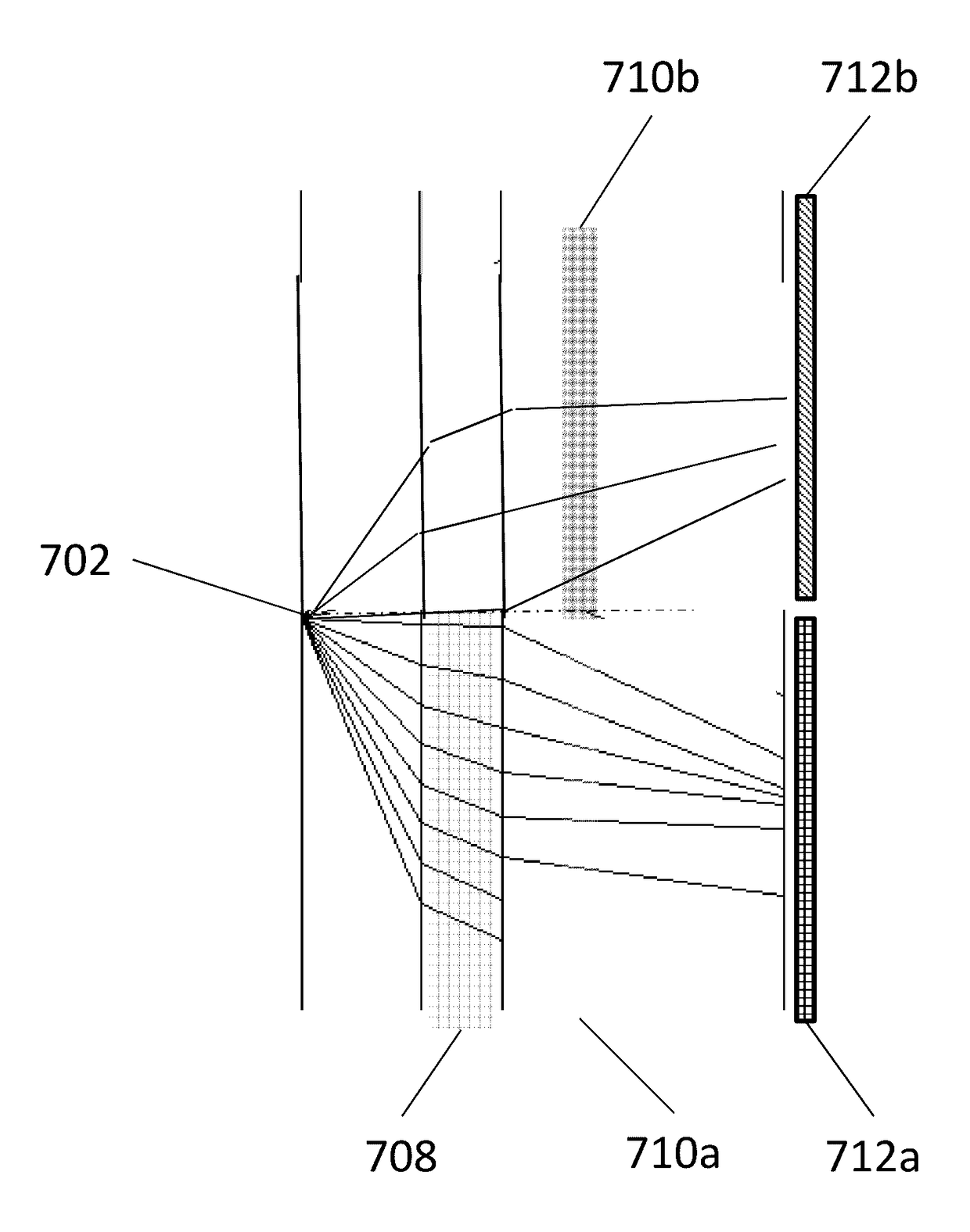
[0174]An exemplary semiconductor fabrication process according to one aspect of the instant invention is shown in FIGS. 26A-26R, which illustrate fabrication of an array of integrated analytical devices comprising a diffractive beam shaping element to spatially separate light emitted from a nanoscale emission volume and direct the spatially-separated light through a plurality of color filters to a plurality of sensing regions within a detector layer.

[0175]In the exemplary methods, the process begins with a clean semiconductor substrate layer, preferably an integrated CMOS detector layer, although the array could be designed to be attached to a separate detector device. Accordingly, the substrate layer can be of any suitable rigid material with sufficient transparency to light emitted from the reaction well. For examples of appropriate detector layers, see CMOS Imagers From Phototransduction to Image Processing (2004) Yadid-Pecht and Etienne-Cummings, eds.; Springer; CMOS / CCD Sensors...


PUM

PropertyMeasurementUnit
thickaaaaaaaaaa
wavelengthsaaaaaaaaaa
thicknessaaaaaaaaaa

Abstract

Arrays of integrated analytical devices and their methods for production are provided. The arrays are useful in the analysis of highly multiplexed optical reactions in large numbers at high densities, including biochemical reactions, such as nucleic acid sequencing reactions. The devices allow the highly sensitive discrimination of optical signals using features such as spectra, amplitude, and time resolution, or combinations thereof. The devices include an integrated diffractive beam shaping element that provides for the spatial separation of light emitted from the optical reactions.

Description

CROSS-REFERENCE TO RELATED APPLICATION[0001]This application claims the benefit of U.S. Provisional Application No. 62 / 042,793, filed on Aug. 27, 2014, the disclosure of which is incorporated herein by reference in its entirety.BACKGROUND OF THE INVENTION[0002]In analytical systems, the ability to increase the number of analyses being carried out at any given time by a given system has been a key component to increasing the utility and extending the lifespan of such systems. In particular, by increasing the multiplex factor of analyses with a given system, one can increase the overall throughput of the system, thereby increasing its usefulness while decreasing the costs associated with that use.[0003]In optical analyses, increasing multiplex often poses increased difficulties, as it can require more complex optical systems, increased illumination or detection capabilities, and new reaction containment strategies. In some cases, systems seek to increase multiplex by many fold, and ev...

Claims


Application Information

Patent Timeline
Patent Type & Authority Patents(United States)
IPC IPC(8): G01N21/78G02B27/42G02B5/28G02B5/18G02B5/20G01N21/77
CPCG01N21/78G02B5/1895G02B5/201G02B5/285G02B27/4238G02B27/4244G01N2201/068G01N2021/7756G01N21/648G01N2021/6478G01N21/6454H01L27/14621H01L27/14627H01L27/14685G01N21/6428G01N21/7703G01N2021/6439G01N2021/7786G01N2201/0873G02B6/132G02B6/136G02B2006/12102G02B2006/12109
Inventor GROT, ANNETTESAXENA, RAVILUNDQUIST, PAUL
Owner PACIFIC BIOSCIENCES
Features
  • R&D
  • Intellectual Property
  • Life Sciences
  • Materials
  • Tech Scout
  • Unparalleled Data Quality
  • Higher Quality Content
  • 60% Fewer Hallucinations
Learn More