AI technical title is built by Patsnap AI team. It summarizes the technical point description of the patent document.
a protection device and shielding technology, applied in semiconductor devices, semiconductor/solid-state device details, diodes, etc., can solve problems such as failure to solve problems, failure to protect a semiconductor integrated circuit from surge, and increase the clamp voltage, so as to reduce the current pathway, suppress the generation of esl, and reduce the current current path
Active Publication Date: 2017-04-25
MURATA MFG CO LTD
View PDF60 Cites 2 Cited by
Summary
Abstract
Description
Claims
Application Information
AI Technical Summary
This helps you quickly interpret patents by identifying the three key elements:
Problems solved by technology
Method used
Benefits of technology
Benefits of technology
[0006]Therefore, an object of the present invention is to provide an ESD protection device which suppresses the ESL, and keeps the clamp voltage low.
[0008]In this configuration, the first and second input / output electrodes of the ESD protection device is formed in closer positions on the semiconductor substrate, and the current pathway of the ESD protection device can be thus shortened. As a result, the generation of ESL can be suppressed, and the increase in clamp voltage can be avoided.
[0010]This configuration makes it easy to mount the ESD protection device onto a substrate, because the first opening and the second opening which serve as external input / output terminals of the ESD protection device are provided at both ends in the longitudinal direction of the semiconductor substrate.
[0012]In this configuration, when currents flow through the two diodes, the current flow in directions opposite to each other, and magnetic fields generated by the current flows thus cancel each other out. For this reason, the inductance of the current pathway is reduced, and lower ESL can be achieved.
[0013]According to the present invention, the shortened current pathway of the ESD protection device can suppress the generation of ESL and keeps the clamp voltage low.
Problems solved by technology
Such semiconductor integrated circuits are low-voltage drive circuits composed of micro wiring patterns formed on semiconductor substrates, and thus generally fragile against electrostatic discharge such as surge.
In particular, in the case of using an ESD protection circuit in the high-frequency band, the clamp voltage is increased as the ESL is increased, and there are thus problems such as failure to protect a semiconductor integrated circuit from surge.
This problem is not able to be solved by Patent Document 1.
Method used
Image
Click on the blue label to locate the original text in one second.
Reading with bidirectional positioning of images and text.
Examples
Embodiment Construction
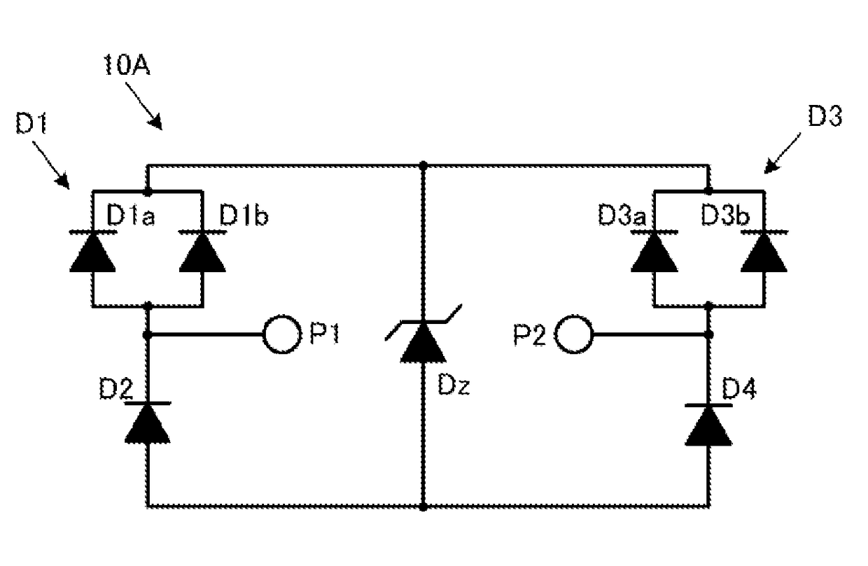
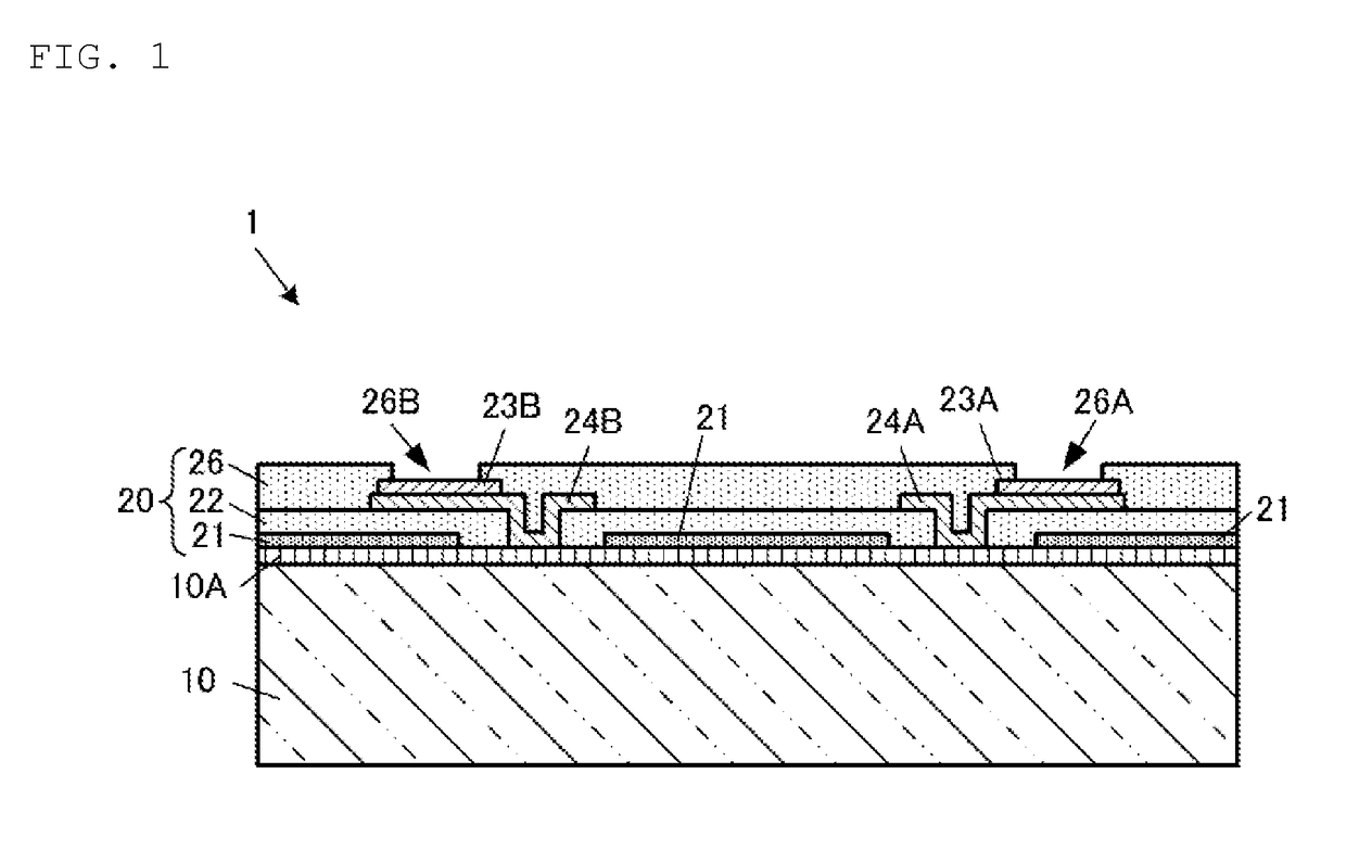
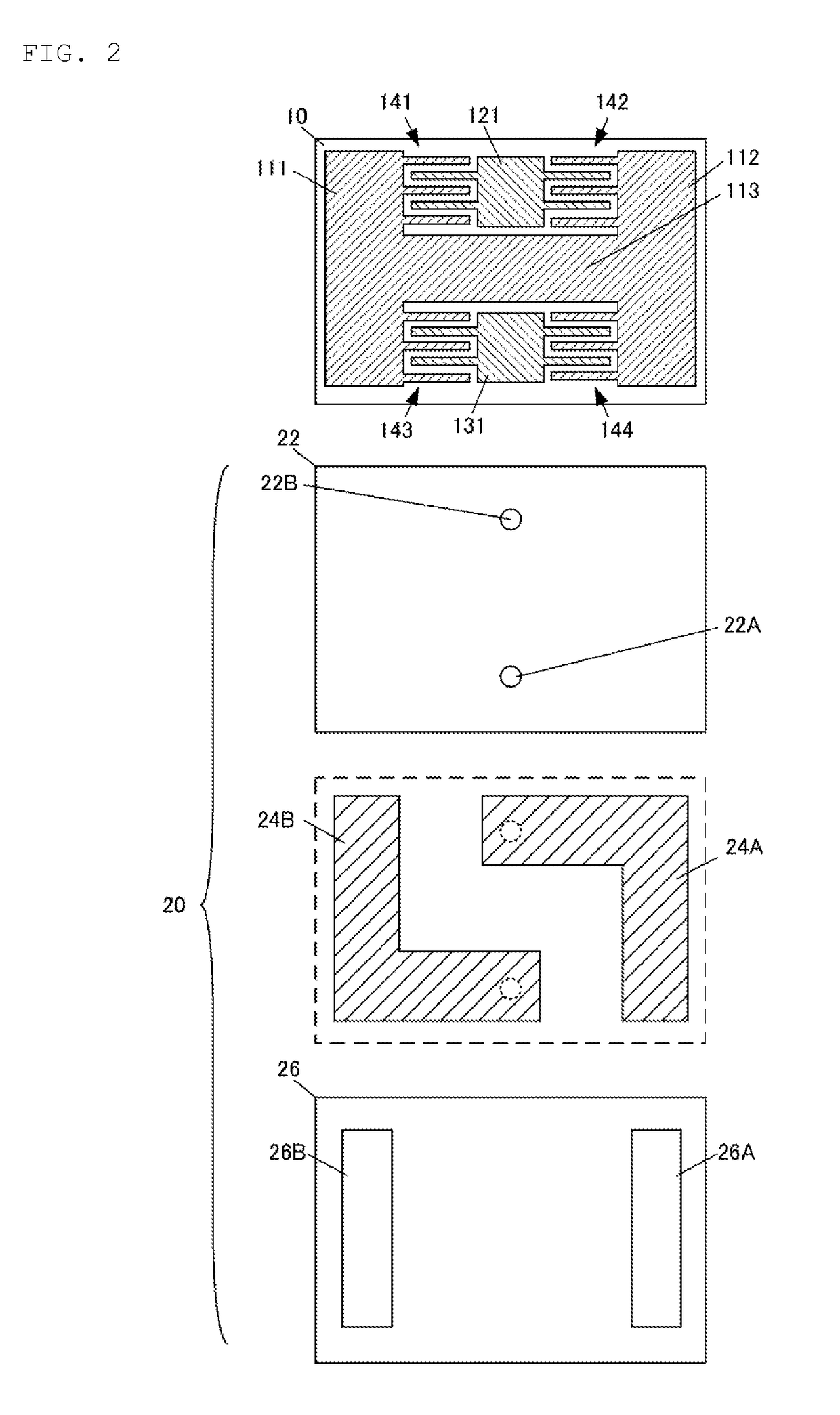
[0029]FIG. 1 is a front cross-sectional view of an ESD protection device 1 according to the present embodiment. FIG. 2 is a plan view of respective layers of the ESD protection device 1. The ESD protection device 1 is a CSP (Chip Size Package) type device, where a rewiring layer 20 including multiple resin layers, etc. is formed on a Si substrate 10. The Si substrate 10 has a rectangular shape with long sides and short sides in planar view, and has an ESD protection circuit 10A configured to include diodes and a zener diode. While the Si substrate 10 corresponds to a semiconductor substrate according to the present invention, the semiconductor substrate according to the present invention is not limited to any Si substrate, but may be a GaAs substrate or the like.
[0030]FIG. 3 is a diagram illustrating the ESD protection circuit 10A formed on the Si substrate 10.
[0031]FIG. 4 is a diagram illustrating a structure example of the ESD protection circuit 10A.
[0032]As shown in FIG. 2, the S...
PUM
Abstract
An ESD protection device includes a zener diode, and a series circuit of diodes and a series circuit of diodes that are connected in parallel with the zener diode. At the connection point between the diodes, an Al electrode film is formed on the surface of a Si substrate, and at the connection point between diodes, an Al electrode film is formed on the surface of the Si substrate. The diodes are formed on the surface of the Si substrate, and the diodes are formed in the thickness direction of the Si substrate. The Si substrate has a longitudinal direction and a shorter direction orthogonal to the longitudinal direction in planar view, and the Al electrode films are formed respectively at both ends in the shorter direction of the Si substrate. Thus, provided is an ESD protection device which suppresses the ESL, and keeps the clamp voltage low.
Description
CROSS REFERENCE TO RELATED APPLICATIONS[0001]The present application is a continuation of PCT / JP2014 / 054404 filed Feb. 25, 2014, which claims priority to JP Application No. 2013-149004, filed Jul. 18, 2013, JP Application No. 2013-126659, filed Jun. 17, 2013, JP Application No. 2013-115676, filed May 31, 2013, JP Application No. 2013-097494, filed May 7, 2013, JP Application No. 2013-079960, filed Apr. 5, 2013, JP Application No. 2013-079978, filed Apr. 5, 2013, and JP Application No. 2013-039379, filed Feb. 28, 2013, the entire contents of each of which are incorporated herein by reference.FIELD OF THE INVENTION[0002]The present invention relates to an ESD protection device which protects an electronic circuit from electrostatic discharge.BACKGROUND OF THE INVENTION[0003]ESD (Electro-Static-Discharge) protection devices can be a type of semiconductor devices. The ESD protection device protects semiconductor ICs, etc. from static electricity, etc. Various electronic devices includin...
Claims
Application Information
Patent Timeline
Application Date:The date an application was filed.
Publication Date:The date a patent or application was officially published.
First Publication Date:The earliest publication date of a patent with the same application number.
Issue Date:Publication date of the patent grant document.
PCT Entry Date:The Entry date of PCT National Phase.
Estimated Expiry Date:The statutory expiry date of a patent right according to the Patent Law, and it is the longest term of protection that the patent right can achieve without the termination of the patent right due to other reasons(Term extension factor has been taken into account ).
Invalid Date:Actual expiry date is based on effective date or publication date of legal transaction data of invalid patent.

