A bidirectional low-voltage planar transient voltage suppression diode and a manufacturing method thereof

A technology of transient voltage suppression and manufacturing method, applied in semiconductor/solid-state device manufacturing, circuits, electrical components, etc., can solve the problem of large reverse leakage current of diodes, reduce leakage current, reduce losses, and reduce short-circuit risks Effect

Active Publication Date: 2018-12-11
西安卫光科技有限公司
View PDF4 Cites 2 Cited by
  • Summary
  • Abstract
  • Description
  • Claims
  • Application Information

AI Technical Summary

Problems solved by technology

[0004] The technical problem to be solved by the present invention is to provide a bidirectional low-voltage planar transient voltage suppression diode and

Method used


Image

  • A bidirectional low-voltage planar transient voltage suppression diode and a manufacturing method thereof
  • A bidirectional low-voltage planar transient voltage suppression diode and a manufacturing method thereof
  • A bidirectional low-voltage planar transient voltage suppression diode and a manufacturing method thereof

Examples


Embodiment 1

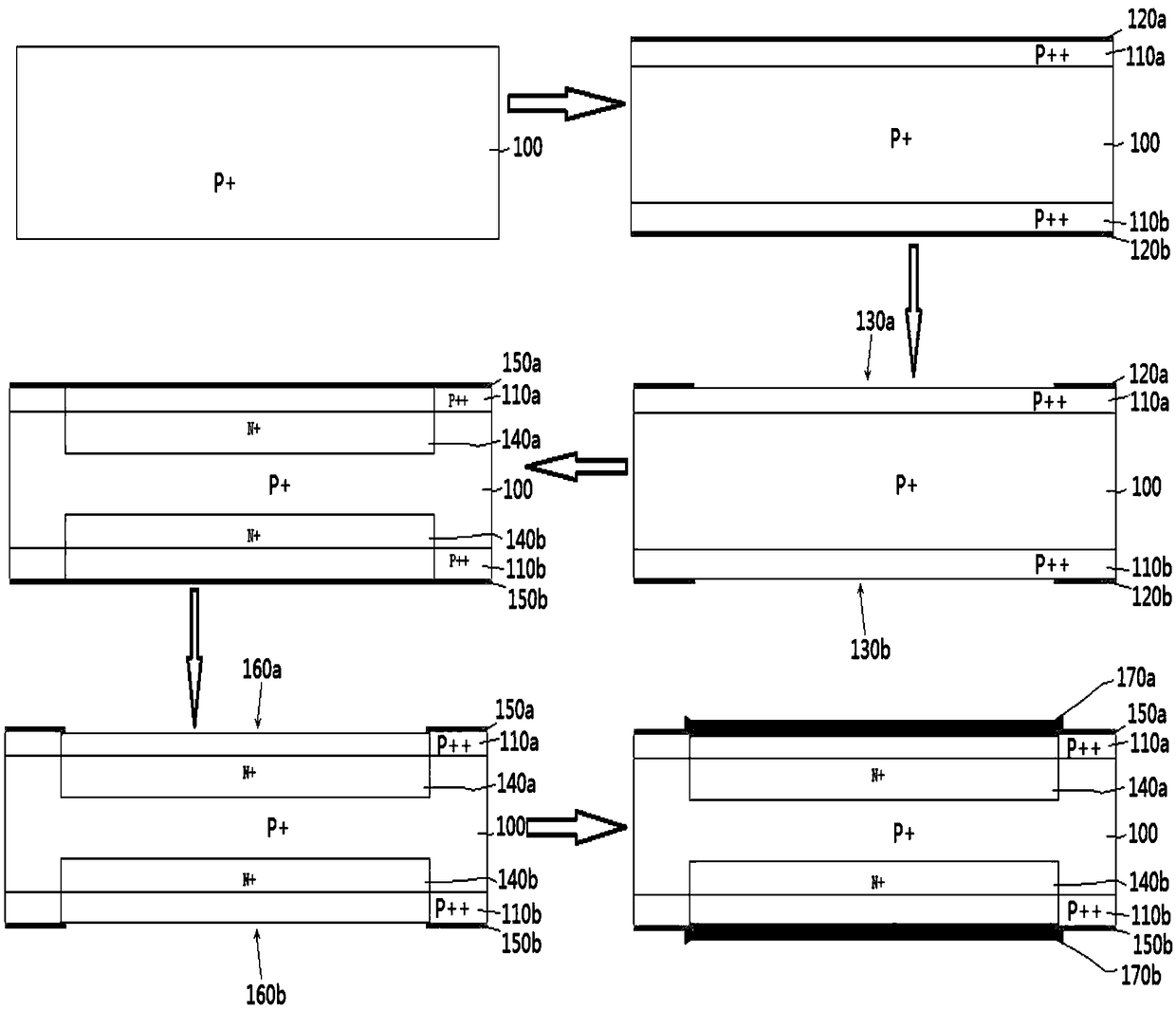
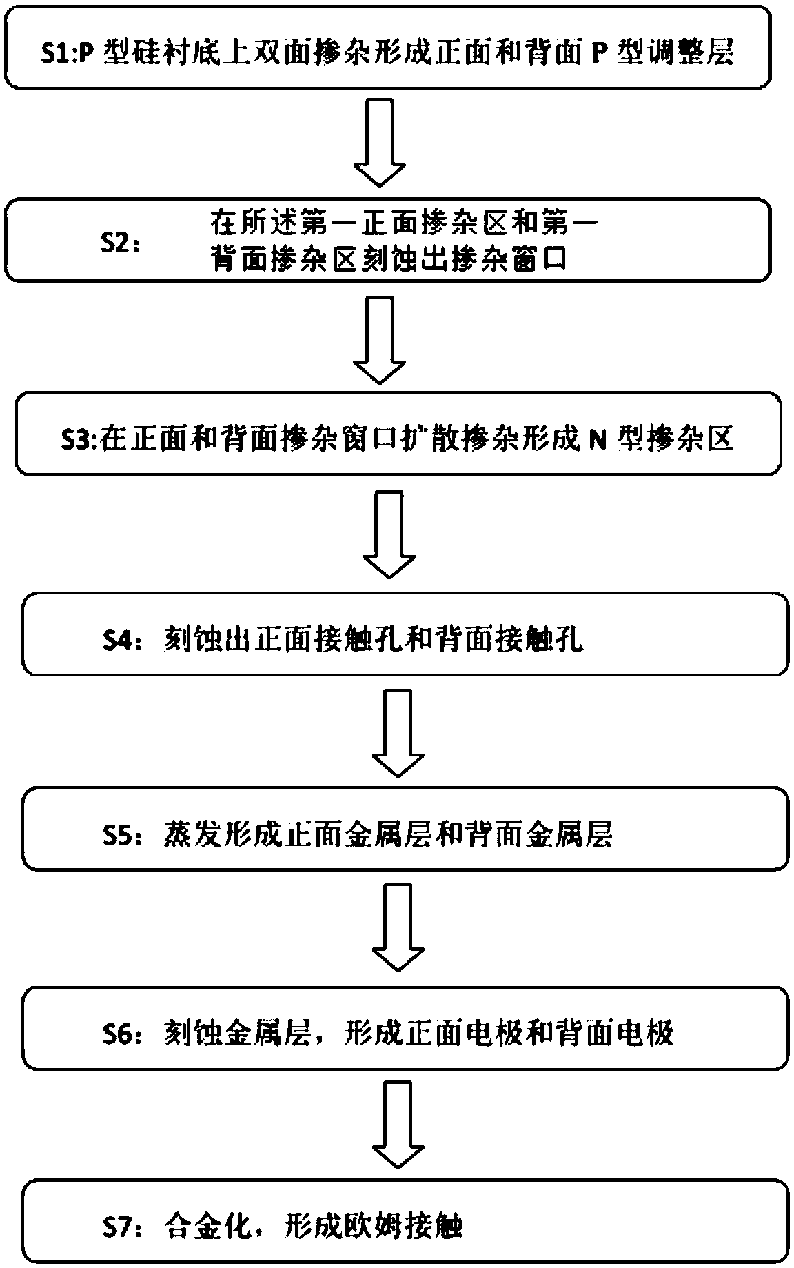
[0047] 1. A heavily doped silicon substrate 100 is provided.

[0048] In this embodiment, the silicon substrate is a P+ silicon substrate. The resistivity of the P+ silicon substrate is between 0.003 Ω·m, 111 crystal orientation, and the thickness is 180 μm.

[0049] 2. Simultaneously diffuse doping to the front and back of the silicon substrate 100 to form a doped region.

[0050] The front doped region of the silicon substrate 100 is called the first front doped region 110a, and the back doped region is called the first back doped region 110b, and the first front doped region 110a and the first back doped region The doping type of the region 110 b is the same as that of the silicon substrate 100 .

[0051] Preferably, diffusion doping adopts two-step diffusion:

[0052] In the first step, prediffusion is performed on the silicon substrate to form a limited B impurity source;

[0053] In the second step, chlorine is added to oxidize when re-diffusion pushes the junction d...

Embodiment 2

[0064] 1. A heavily doped silicon substrate 100 is provided. The P+ silicon substrate has a resistivity of 0.01Ω·m, a 111 crystal orientation, and a thickness of 200 μm.

[0065] 2. Simultaneously diffuse doping to the front and back of the silicon substrate 100 to form a first front doped region 110a and a first back doped region 110b, the first front doped region 110a and the first back doped region 110b The doping type is the same as that of the silicon substrate 100 .

[0066] A two-step diffusion doping is employed:

[0067] In the first step, prediffusion is performed on the silicon substrate to form a limited B impurity source;

[0068] In the second step, chlorine is added to oxidize when re-diffusion pushes the junction deep.

[0069] While doping to form the doped region, a first front oxide layer 120a is formed on the first front doped region 110a, and a first rear oxide layer 120b is formed on the first back doped region 110b. The first front doped region 110a ...

Embodiment 3

[0079] 1. A heavily doped silicon substrate 100 is provided. The resistivity of the P+ silicon substrate is between 0.02 Ω·m, 111 crystal orientation, and the thickness is 240 μm.

[0080] 2. Simultaneously diffuse doping to the front and back of the silicon substrate 100 to form a first front doped region 110a and a first back doped region 110b, the first front doped region 110a and the first back doped region 110b The doping type is the same as that of the silicon substrate 100 .

[0081] A two-step diffusion doping is employed:

[0082] In the first step, prediffusion is performed on the silicon substrate to form a limited B impurity source;

[0083] In the second step, chlorine is added to oxidize when re-diffusion pushes the junction deep.

[0084] While doping to form the doped region, a first front oxide layer 120a is formed on the first front doped region 110a, and a first rear oxide layer 120b is formed on the first back doped region 110b. The first front doped re...


PUM

PropertyMeasurementUnit
Thicknessaaaaaaaaaa
Resistivityaaaaaaaaaa
Thicknessaaaaaaaaaa

Abstract

The invention discloses a bidirectional low-voltage planar transient voltage suppression diode and a manufacturing method thereof, comprising a P-type heavily doped silicon substrate; A first front doping region and a first back doping region are respectively formed on the front and back sides of the substrate, A second front doping region and a second back doping region are respectively formed bydiffusion doping through a doping window on the front surface and the back surface of the substrate, a second front doped region oxide layer and a second back doped region oxide layer are formed on the second front doped region and the second back doped region, respectively, a front contact hole and a back contact hole are formed on the second front doped region oxide layer and the second back doped region oxide layer; A front metal electrode and a back metal electrode are formed on the front contact hole and the back contact hole, respectively. A front doping region and a back doping regionwith the same doping type as the silicon substrate are added so as to adjust the substrate concentration, thereby increasing the concentration gradient across the formed PN junction, reducing the movable ions and reducing the TVS leakage current.

Description

【Technical field】 [0001] The invention belongs to the technical field of semiconductor components, and in particular relates to a bidirectional low-voltage planar transient voltage suppression diode chip and a manufacturing method thereof. 【Background technique】 [0002] Transient voltage suppression diodes (TVS) have been widely used in the protection of circuits, network ports, and precision devices from static electricity, surges, and lightning strikes. Most manufacturers at home and abroad use pickling (OJ) or glass passivation (GPP) countertop technology to manufacture TVS. [0003] In comparison, the use of planar technology to manufacture TVS does not require slotting and coating glass powder, the process equipment is simple, the processing cycle is short, and the process stability and consistency are superior. However, TVS with lower voltage is manufactured by planar technology, especially when the breakdown voltage is less than 10V, because the breakdown of PN junc...

Claims


Application Information

Patent Timeline
IPC IPC(8): H01L29/06H01L29/45H01L29/861H01L21/285H01L21/329
CPCH01L21/2855H01L29/0638H01L29/0684H01L29/456H01L29/66136H01L29/8613
Inventor 李家贵
Owner 西安卫光科技有限公司
Why Eureka
Try Eureka