Semiconductor device with diode and silicon controlled rectifier (SCR)

a technology of diodes and rectifiers, applied in semiconductor devices, diodes, transistors, etc., can solve the problems of increasing the clamping voltage of the device accordingly, slow operation speed, damage to the integrated circuit, etc., and achieves low capacitance, fast turn-on, and small area

Active Publication Date: 2020-11-19
UPI SEMICON CORP
View PDF0 Cites 2 Cited by
  • Summary
  • Abstract
  • Description
  • Claims
  • Application Information

AI Technical Summary

Benefits of technology

[0014]Based on the above, in the present invention, a diode and a silicon controlled rectifier (SCR) are integrated into a bypass diode structure in a transient voltage suppressor (TVS). The hybrid structure not only has the advantages of the diode including small area, low capacitance, and fast turn-on, but also has the characteristics of the SCR including high current gain and low clamping voltage, thereby achieving better ESD protection effect.

Problems solved by technology

Electrostatic discharge (ESD) events are one of the main problems that cause damage to integrated circuits.
When the area of the PN junction is larger, the parasitic capacitance is also larger, which leads to a slower operation speed.
On the other hand, if a small-area diode structure is selected to reduce parasitic capacitance, the resistance value of the device will increase, thereby increasing the clamping voltage of the device accordingly, which will cause the ESD protection capability to decrease.

Method used


Image

  • Semiconductor device with diode and silicon controlled rectifier (SCR)
  • Semiconductor device with diode and silicon controlled rectifier (SCR)
  • Semiconductor device with diode and silicon controlled rectifier (SCR)

Examples


first embodiment

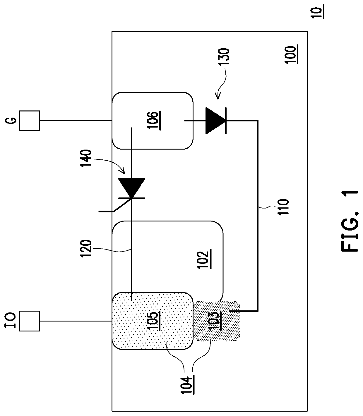
[0025]FIG. 1 is a schematic cross-sectional view of a semiconductor device according to the invention.

[0026]Referring to FIG. 1, in the first embodiment, a semiconductor device 10 includes a substrate 100, a well region 102, a first doped region 104, and a second doped region 106. In one embodiment, the substrate 100 may be a semiconductor substrate, a semiconductor compound substrate, or a semiconductor over insulator (SOI) substrate, for example. In the present embodiment, the substrate 100 may have a first conductivity type, which may be an N-type silicon substrate and electrically floating, for example.

[0027]The well region 102 may have a second conductivity type and is disposed in the substrate 100. In one embodiment, the dopant of the well region 102 may be boron or boron difluoride. For example, the well region 102 may be a P-type well region and is electrically floating.

[0028]The first doped region 104 may have the first conductivity type and is disposed in the substrate 100...

second embodiment

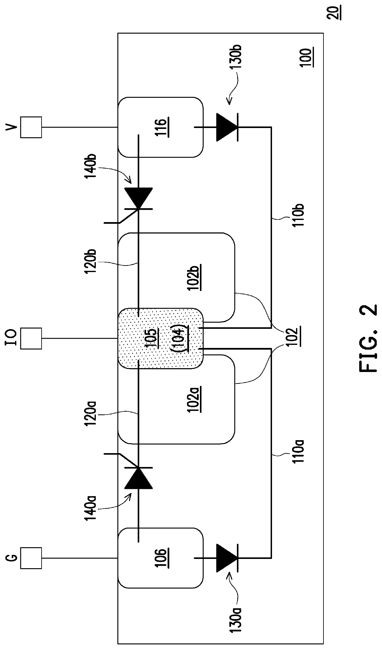
[0031]FIG. 2 is a schematic cross-sectional view of a semiconductor device according to the invention.

[0032]Referring to FIG. 2, in the second embodiment, a semiconductor device 20 includes a substrate 100 having a first conductivity type, a well region 102 having a second conductivity type, a first doped region 104 having the first conductivity type, and a second doped region having the second conductivity type 106, and a third doped region 116 having the second conductivity type.

[0033]Specifically, the well region 102 is divided into a first well region 102a and a second well region 102b by the first doped region 104. That is, the well region 102 has the first well region 102a and the second well region 102b separated from each other, the first doped region 104 is located between the first well region 102a and the second well region 102b, and the first doped region 104 is in contact with the first well region 102a and the second well region 102b respectively to form PN junctions. ...

third embodiment

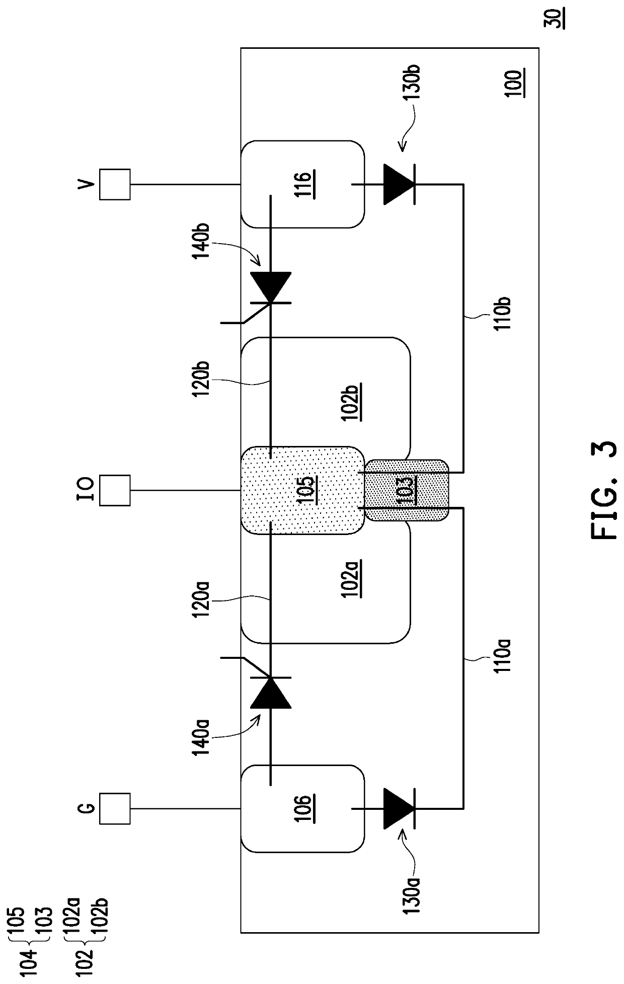
[0036]FIG. 3 is a schematic cross-sectional view of a semiconductor device according to the invention.

[0037]Referring to FIG. 3, a semiconductor device 30 of the third embodiment is similar to the semiconductor device 20 of the second embodiment. A difference there-between is that the first doped region 104 of the semiconductor device 30 of the third embodiment includes a first doped sub-region 103 and a second doped sub-region 105 located on the first doped sub-region 103. The first doped sub-region 103 may have a bottom surface lower than the bottom surfaces of the first and second well regions 102a and 102b. That is, the first doped sub-region 103 (or the first doped region 104) protrudes from the bottom surfaces of the first and second well regions 102a and 102b, so as to contact the substrate 100. In the structure, a current at the ground terminal G may flow from the current path 110a of the diode 130a or the current path 120a of the silicon controlled rectifier 140a to the inp...


PUM

PropertyMeasurementUnit
conductivity typeaaaaaaaaaa
electrically floatingaaaaaaaaaa
currentaaaaaaaaaa

Abstract

Provided is a semiconductor device with a diode and a silicon controlled rectifier (SCR) including a substrate having a first conductivity type, a well region having a second conductivity type, a first doped region having the first conductivity type, and a second doped region having the second conductivity type. The well region is disposed in the substrate. The first doped region is disposed in the substrate. The second doped region is disposed in the substrate. The well region and the first doped region form a first PN junction, the well region and the substrate form a second PN junction, and the substrate and the second doped region form a third junction. The first, second, and third PN junctions form the SCR, and the first doped region and the third PN junction form the diode.

Description

CROSS-REFERENCE TO RELATED APPLICATION[0001]This application claims the priority benefit of Taiwan application serial no. 108116674, filed on May 15, 2019. The entirety of the above-mentioned patent application is hereby incorporated by reference herein and made a part of this specification.BACKGROUND OF THE INVENTIONField of the Invention[0002]The present invention relates to a semiconductor device with a diode and a silicon controlled rectifier (SCR).Description of Related Art[0003]With the rapid development of current technology, integrated circuits are widely used in electronic devices. Electrostatic discharge (ESD) events are one of the main problems that cause damage to integrated circuits.[0004]In the conventional technical field, transient voltage suppressors (TVS) are often used for electrostatic discharge protection. However, since the transient voltage suppressors need to withstand high power energy, its bypass diode must be designed with a large area of PN junction to wi...

Claims


Application Information

Patent Timeline
Patent Type & Authority Applications(United States)
IPC IPC(8): H01L29/74H01L29/747H01L27/02
CPCH01L29/747H01L29/7412H01L27/0262H01L27/0255H01L29/861H01L29/87
Inventor CHEN, CHIH-HAO
Owner UPI SEMICON CORP
Why Eureka
Try Eureka