Unidirectional high-voltage transient voltage suppression protection device and preparation method thereof

A technology for transient voltage suppression and device protection, applied in semiconductor/solid-state device manufacturing, electric solid-state devices, electrical components, etc., can solve the problems of large dynamic impedance, high clamping voltage, low clamping voltage, etc., and achieve dynamic impedance The effect of small, low clamping voltage

Pending Publication Date: 2020-09-15
WILL SEMICON (SHANGHAI) CO LTD
View PDF0 Cites 2 Cited by
  • Summary
  • Abstract
  • Description
  • Claims
  • Application Information

AI Technical Summary

Problems solved by technology

[0002] As the charging speed of electronic products continues to accelerate, the charging power and charging voltage are higher, and electronic products have higher requirements for the protection ability of ESD (electrostatic discharge) and EOS (electrical overstress), and the requirements for higher operating voltage are relatively low. Clamping voltage and dynamic impedance, the current higher working voltage unidirectional transient voltage suppression protection device products are all avalanche breakdown diodes, this kind of common structure diode has the disadvantages of high clamping voltage and large dynamic impedance

Method used


Image

  • Unidirectional high-voltage transient voltage suppression protection device and preparation method thereof
  • Unidirectional high-voltage transient voltage suppression protection device and preparation method thereof
  • Unidirectional high-voltage transient voltage suppression protection device and preparation method thereof

Examples


Embodiment Construction

[0025] In order to make the purpose, technical solutions and advantages of the embodiments of the present invention clearer, the technical solutions in the embodiments of the present invention will be clearly and completely described below in conjunction with the drawings in the embodiments of the present invention. Obviously, the described embodiments It is a part of embodiments of the present invention, but not all embodiments. Based on the embodiments of the present invention, all other embodiments obtained by persons of ordinary skill in the art without creative efforts fall within the protection scope of the present invention.

[0026] Various non-limiting embodiments of the present invention will be described in detail below in conjunction with the accompanying drawings.

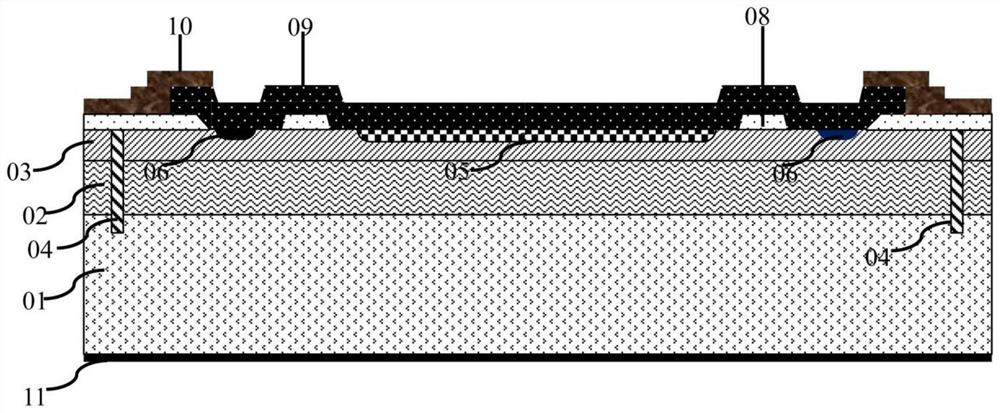
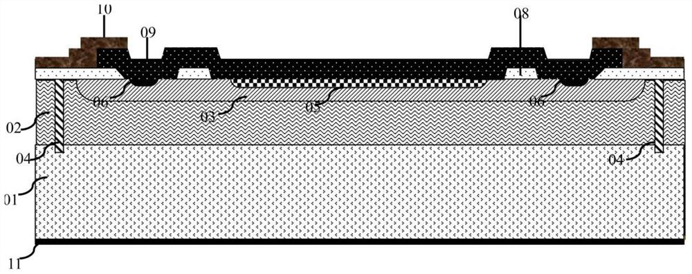
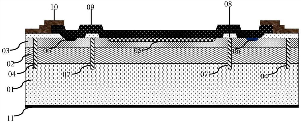
[0027] In order to understand the structure and function of a unidirectional high-voltage transient voltage suppression protection device provided by an embodiment of the present invention in more deta...


PUM


Abstract

An unidirectional high-voltage transient voltage suppression protection device comprises a substrate of a first conductive type; a first epitaxial layer of a second conductivity type, the first epitaxial layer being formed over the top surface of the substrate; a semiconductor layer in a second conductivity type, the semiconductor layer being a well region formed in the top surface of the first epitaxial layer or a second epitaxial layer formed above the top surface of the first epitaxial layer; a group of first injection regions and second injection regions formed in the top surface of the semiconductor layer, the first injection region being formed on the periphery of the second injection region, and the first injection region and the second injection region being horizontally spaced bya preset distance; and a first isolation groove on the periphery of the first injection region, the first isolation groove being formed in the substrate, the first epitaxial layer and the semiconductor layer, and the first isolation groove being filled with an insulating material. The embodiment of the invention provides a unidirectional high-working-voltage transient voltage suppression protection device of a transient voltage suppression protection device.

Description

technical field [0001] The embodiments of the present invention relate to the technical field of integrated circuits, and in particular to a unidirectional high-voltage transient voltage suppression protection device and a preparation method thereof. Background technique [0002] As the charging speed of electronic products continues to accelerate, the charging power and charging voltage are higher, and electronic products have higher requirements for the protection ability of ESD (electrostatic discharge) and EOS (electrical overstress), and the requirements for higher operating voltage are relatively low. The clamping voltage and dynamic impedance of the existing higher working voltage unidirectional transient voltage suppression protection device products are all avalanche breakdown diodes. The diodes with this common structure have the disadvantages of high clamping voltage and large dynamic impedance. [0003] It is against this background that the technical solution of...

Claims


Application Information

Patent Timeline
IPC IPC(8): H01L27/02H01L21/82
CPCH01L27/0255H01L27/0259H01L21/82
Inventor 张富生许成宗韩业星
Owner WILL SEMICON (SHANGHAI) CO LTD
Why Eureka
Try Eureka