Method and apparatus for inspection of light emitting semiconductor devices using photoluminescence imaging

a technology of light-emitting semiconductors and methods, applied in the direction of fluorescence/phosphorescence, instruments, television systems, etc., can solve the problems of requiring additional tools, slow probing, and damage to leds, and achieve the effect of fast and contactless inspection

Active Publication Date: 2017-05-02
KLA CORP
View PDF22 Cites 1 Cited by
  • Summary
  • Abstract
  • Description
  • Claims
  • Application Information

AI Technical Summary

Benefits of technology

[0010]It is an object of the invention to provide a method to quickly and reliably measure the light power emitted by an LED during a production process. Furthermore, the method should be easy to use, and should not influence or destroy the LED being measured.
[0012]It is a further object of the invention to provide an apparatus to inspect the light power emitted by an LED during a production process. Furthermore, the apparatus should be easy to use, and should not influence or destroy the LED being measured.
[0014]For defect inspection, the photoluminescence effect is used as a kind of back light. This illumination effect enables the finding of defects that are buried, or at least are not visible with normal inspection. With the inventive setup, it is possible to find cuts (finger cuts) or interrupts in the metallization layer. Additionally, the invention allows for the detection of non-homogeneities of the LEDs. The light emitted from the LED is subjected to a spatial gray value analysis. Some LEDs only emit light in some parts, emitting no light in other parts (for example: a dark edge at the corner of the LED does not light up).
[0026]This invention would allow for fast and contactless inspection of light emitting semiconductor devices on an inspection tool widely used by LED manufactures for other inspection tasks.

Problems solved by technology

This has several disadvantages: LEDs may get damaged during probing, probing is slow, and probing requires an additional tool.

Method used


Image

  • Method and apparatus for inspection of light emitting semiconductor devices using photoluminescence imaging
  • Method and apparatus for inspection of light emitting semiconductor devices using photoluminescence imaging
  • Method and apparatus for inspection of light emitting semiconductor devices using photoluminescence imaging

Examples


Embodiment Construction

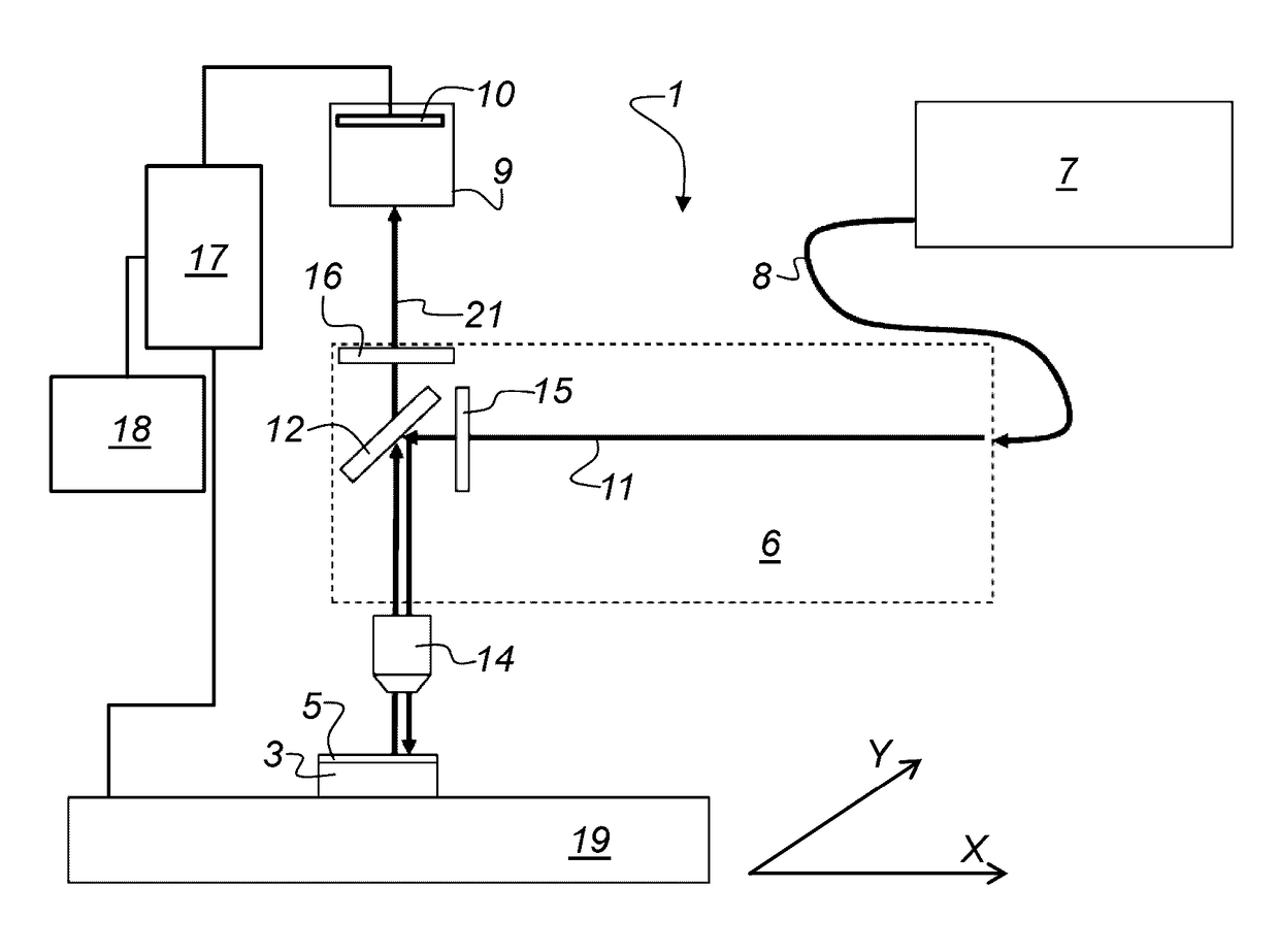
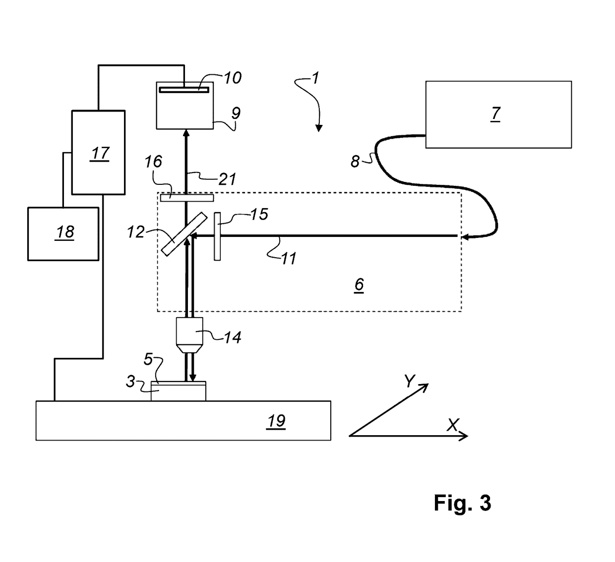
[0036]It is noted the same reference numerals refer to the same elements throughout the various figures. Furthermore, only reference numerals necessary for the description of the respective figure are shown in the figures. The shown embodiments represent only examples of how the invention can be carried out and should not be regarded as limiting the invention. The description below refers to LED die / chips, which should not be regarded as limiting the invention. It should be evident for any person skilled in the art that the present invention is applicable to light emitting semiconductor material in general.

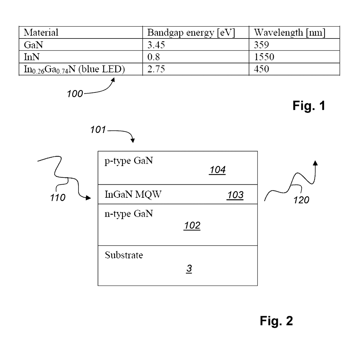
[0037]FIG. 1 is a table 100 showing a bandgap and corresponding wavelength of a III-N semiconductor material system. All semiconductor materials exhibit the so-called photoluminescence effect. This effect is seen when the material is illuminated with light of a certain wavelength and the photons in the light beam raise electrons from a low energy state to a high energy state (gene...


PUM

PropertyMeasurementUnit
wavelengthaaaaaaaaaa
energy levelaaaaaaaaaa
wavelengthaaaaaaaaaa

Abstract

A method and apparatus for the inspection of light emitting semiconductor devices. The semiconductor device is illuminated with a light source, wherein at least an area of the light emitting semiconductor is illuminated with a waveband of light. The waveband of light λA+λB can generate electron-hole pairs in the light emitting semiconductor to be inspected. Through an objective lens at least a part of the light λC emitted by the light emitting semiconductor is detected. The emitted light is captured with a sensor of a camera that is sensitive to wavelengths of the emitted light, wherein the wavelength of the emitted light is above the width of the waveband. The data of the emitted light, captured with the sensor, are transmitted to a computer system for calculating inspection results of the light emitting semiconductor.

Description

CROSS REFERENCE TO RELATED APPLICATIONS[0001]This patent application claims priority to U.S. provisional patent application No. 61 / 500,987 filed Jun. 24, 2011, incorporated herein by reference.FIELD OF THE INVENTION[0002]The present invention relates to a method for inspecting light emitting semiconductor devices during and after a production process. The light emitting semiconductor devices can be LEDs.[0003]The present invention also relates to an apparatus for inspecting light emitting semiconductor devices on a substrate.BACKGROUND OF THE INVENTION[0004]Solid state lighting (SSL) has several advantages compared to conventional lighting, including low power consumption, long lifetime, and small form factor. An important element of SSL is the LED (Light-Emitting Diode) die / chip. The basis for the LED is a semiconductor material that undergoes a complex production process. Several metrology and inspection steps are done during and after the production process of the LED.[0005]Measu...

Claims


Application Information

Patent Timeline
Patent Type & Authority Patents(United States)
IPC IPC(8): G01R31/265G01N21/64H01L33/00G01R31/26
CPCG01R31/2635G01N21/6489G01R31/2656H01L33/0095
Inventor BOEYKENS, STEVENMARIVOET, TOM
Owner KLA CORP
Why Eureka
Try Eureka