Transistor with shield structure, packaged device, and method of manufacture

a shield structure and transistor technology, applied in the field of field effect transistors, can solve the problems of reducing amplifier stability and reducing gain

Active Publication Date: 2017-05-16
NXP USA INC
View PDF13 Cites 38 Cited by
  • Summary
  • Abstract
  • Description
  • Claims
  • Application Information

AI Technical Summary

Problems solved by technology

The tapping of the gate runner can add parasitic feedback cap

Method used


Image

  • Transistor with shield structure, packaged device, and method of manufacture
  • Transistor with shield structure, packaged device, and method of manufacture
  • Transistor with shield structure, packaged device, and method of manufacture

Examples


Embodiment Construction

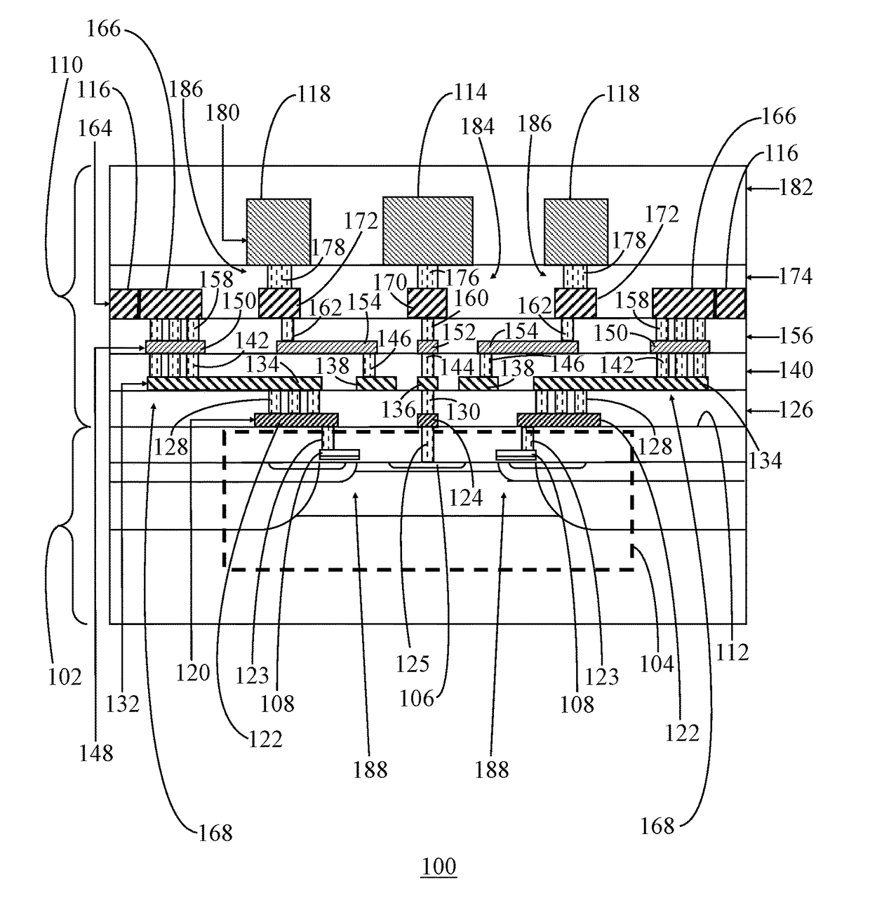
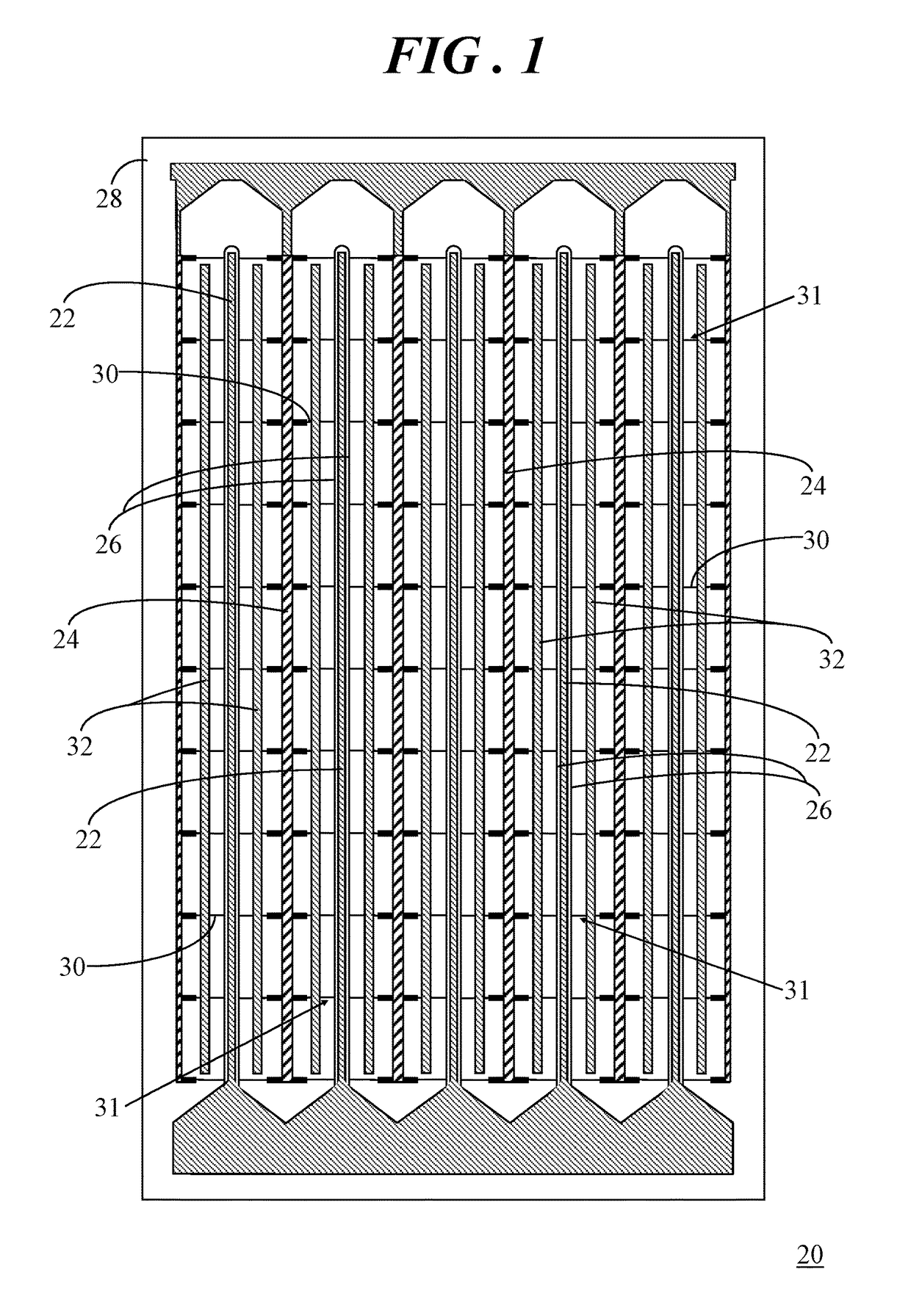
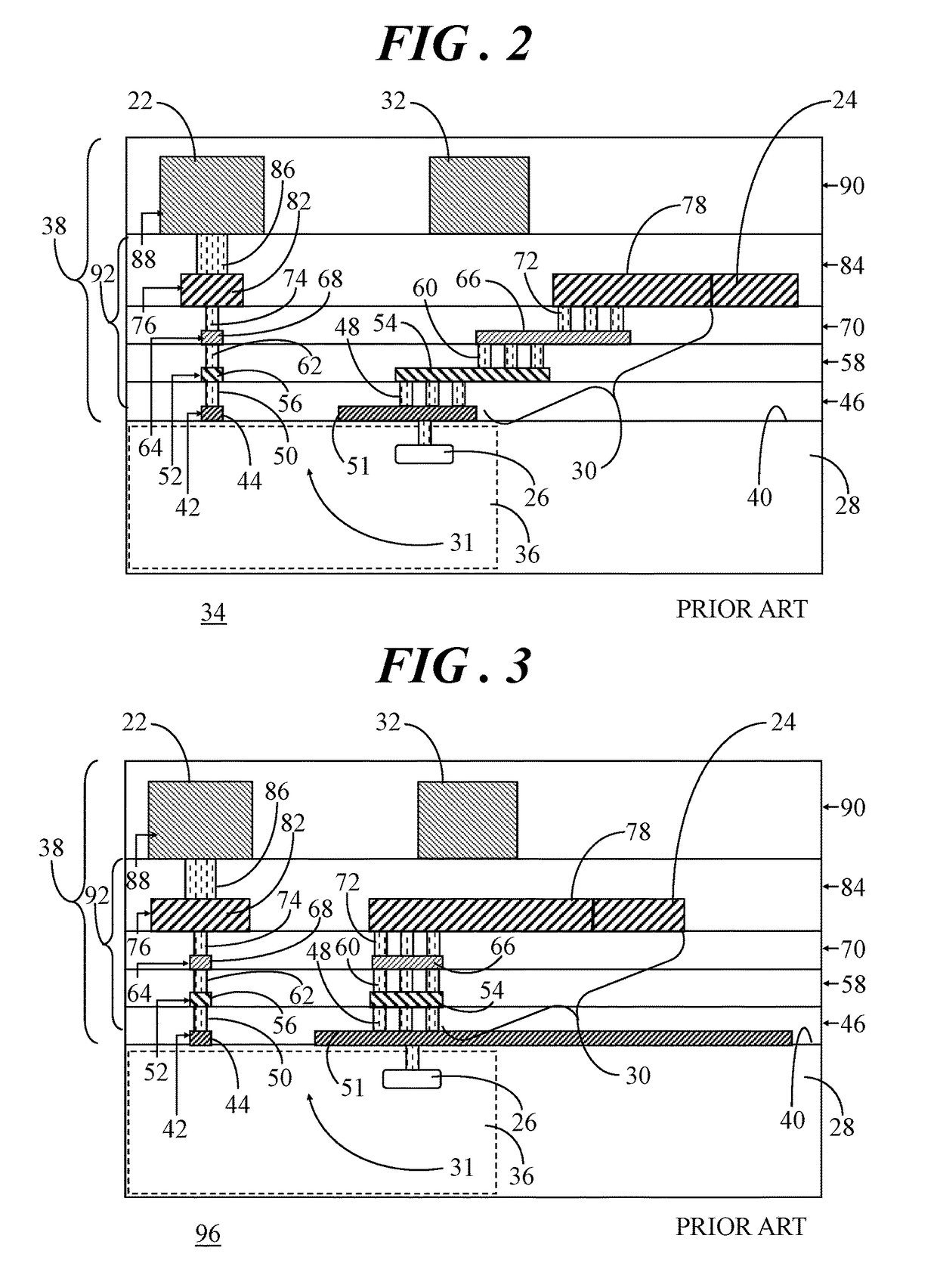
[0016]In overview, embodiments disclosed herein entail a transistor, having a shield structure within an interconnect structure of the transistor, a packaged semiconductor device having such a transistor, and a method of manufacturing the transistor. More specifically, embodiments can include multiple shield structures strategically located along the runners of a multiple runner interdigitated transistor near positions where the input interconnections approach the output interconnections (tap locations). The shield structure includes several layers of grounded electrically conductive material, i.e., metal, and vias extending through the interconnect structure to block electric fields between the input signal tapped from a first runner and the output signal carried to a second runner of the transistor. The geometry of the shield structure is configured to be small to minimize additional input and output capacitance contributions from the shield structure. The geometry of the shield s...


PUM


Abstract

A transistor includes a semiconductor substrate having an intrinsic active device, a first terminal, and a second terminal. The transistor also includes an interconnect structure formed of multiple layers of dielectric material and electrically conductive material on an upper surface of the semiconductor substrate. The interconnect structure includes a pillar, a tap interconnect, and a shield structure formed from the electrically conductive material. The pillar electrically contacts the first terminal, extends through the dielectric material, and connects to a first runner. The tap interconnect electrically contacts the second terminal, extends through the dielectric material, and connects to a second runner. The shield structure extends from a shield runner through the dielectric material toward the semiconductor substrate. The shield structure is positioned between the pillar and the tap interconnect to limit feedback capacitance between the tap interconnect and the pillar.

Description

TECHNICAL FIELD OF THE INVENTION[0001]The present invention relates generally to field effect transistors. More specifically, the present invention relates to a field effect transistor having a shield structure between the input and output of the active device, a packaged semiconductor device with the field effect transistor therein, and a method of manufacturing such a field effect transistor.BACKGROUND OF THE INVENTION[0002]A typical high power semiconductor device package may include one or more input leads, one or more output leads, one or more transistors, wirebonds coupling the input lead(s) to the transistor(s), and wirebonds coupling the transistor(s) to the output lead(s). A field effect transistor (FET) in such a high power semiconductor device package may include interdigitated drain and gate runners. The gate of the FET is driven by an input signal tapped from the gate runner. The tapping of the gate runner can add parasitic feedback capacitance that may reduce amplifier...

Claims


Application Information

Patent Timeline
IPC IPC(8): H01L23/58H01L21/3205H01L21/768H01L21/8234H01L27/02H01L23/522H01L23/66H01L23/552H01L23/528
CPCH01L23/552H01L23/528H01L23/5226H01L23/66H01L27/0203H01L21/823475H01L21/32051H01L21/76802H01L21/76877H01L2223/6644H01L23/522H01L23/535H01L29/0688H01L2224/49175H01L23/4824H01L23/5225H01L2223/6611H01L24/48H01L24/49H01L2224/48247H01L2224/48091H01L2224/48195H01L2924/00014H01L29/7816H01L2224/45099
Inventor HOLMES, DAMONBURDEAUX, DAVIDCHAKRABORTY, PARTHAKHALIL, IBRAHIMRUEDA, HERNAN
Owner NXP USA INC
Why Eureka
Try Eureka