Semiconductor device

a technology of semiconductor devices and dielectric devices, applied in the direction of dielectric devices, semiconductor devices, electrical apparatus, etc., can solve the problems of deterioration of sbd characteristics, achieve small resistance value, improve the reverse surge withstand capability of semiconductor devices, and flow surge current reliable

Active Publication Date: 2017-05-16
SHINDENGEN ELECTRIC MFG CO LTD
View PDF16 Cites 0 Cited by
  • Summary
  • Abstract
  • Description
  • Claims
  • Application Information

AI Technical Summary

Benefits of technology

[0016]According to the semiconductor device of the present invention, a part of the side surface of the second portion and the bottom surface thereof connected to the side surface is in contact with a part of the first portion. Thereby, a thickness from the other main surface of the semiconductor substrate to a Schottky junction surface of the Schottky junction between the bottom surface of the second region and the semiconductor substrate is smaller than a thickness from the other main surface of the semiconductor substrate to the one main surface of the semiconductor substrate in which the first portion is formed. Thereby, a resistance value of the semiconductor substrate at the Schottky junction can be made smaller than a resistance value of the portion of the semiconductor substrate where the first portion is formed. Therefore, it is possible to reliably flow surge current toward the Schottky junction with a small resistance value. As a result, it becomes possible to improve the reverse surge withstand capability of the semiconductor device.

Problems solved by technology

There is a concern that if the reverse voltage exceeds the breakdown voltage limit, the characteristics of the SBD deteriorate.

Method used


Image

  • Semiconductor device
  • Semiconductor device
  • Semiconductor device

Examples


first embodiment

(1) First Embodiment of Schottky Junction

[0036]FIG. 14 is a fragmentary cross-sectional view along the Z-axis direction showing an embodiment of the peripheral region of the Schottky barrier diode that is an example of the semiconductor device according to the present invention.

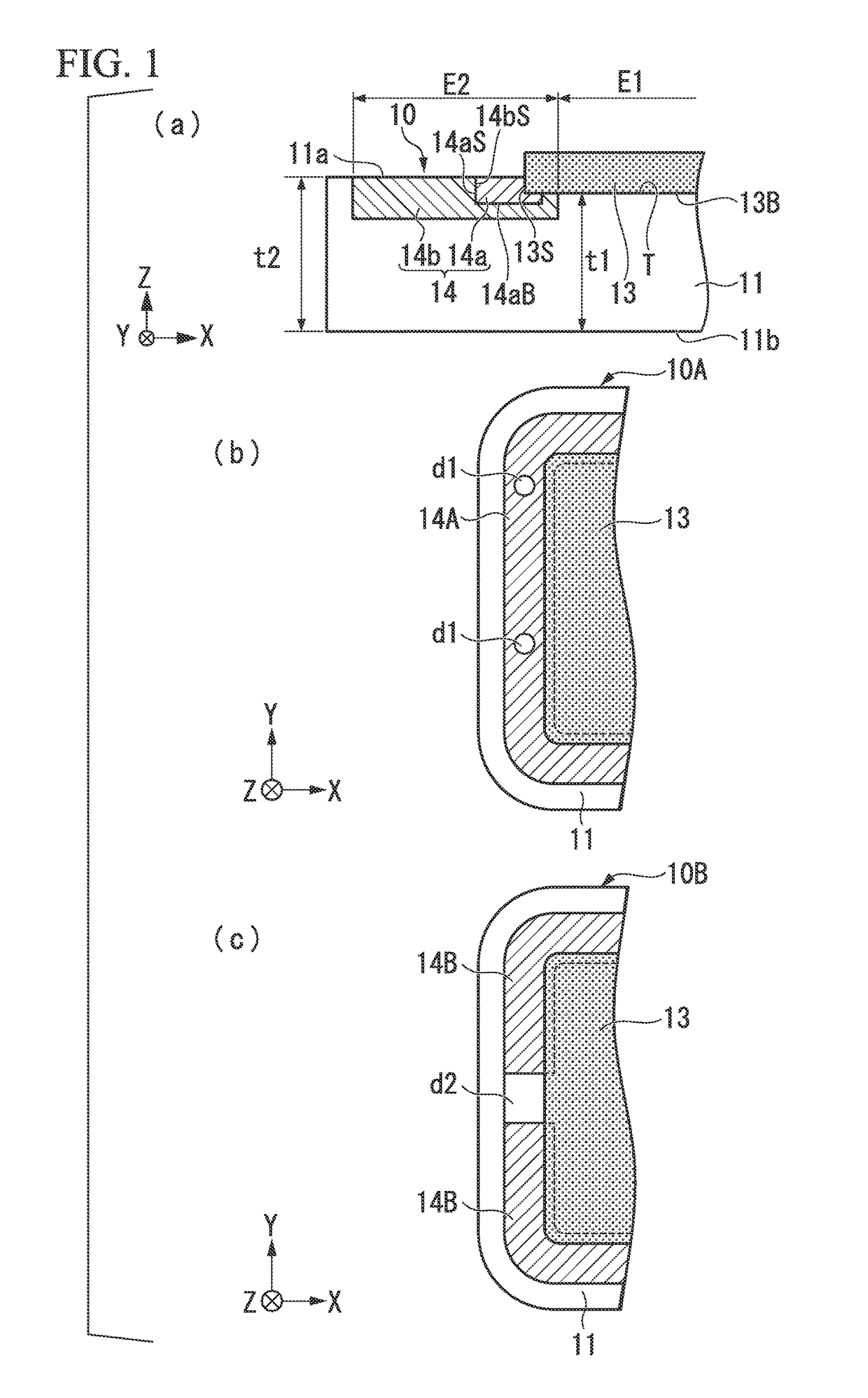
[0037]A Schottky barrier diode (semiconductor device) 10 according to the present embodiment includes at least: a semiconductor substrate 11 (first semiconductor region 12) of n-type (first conductivity type); a p-type semiconductor portion (first portion) 14 of p-type (second conductivity type) opposite to the n-type, which is formed in a part, on the one main surface 11a side, of the semiconductor substrate 11; and a conductive metal portion (second portion) 13 formed on the one main surface 11a side of the semiconductor substrate 11 so as to be electrically connected to a part of the p-type semiconductor portion 14. Additionally, a part of a side surface 13S of the metal portion 13 and a part of a bottom s...

second embodiment

(3) Modified Examples of Second Embodiment of Schottky Junction

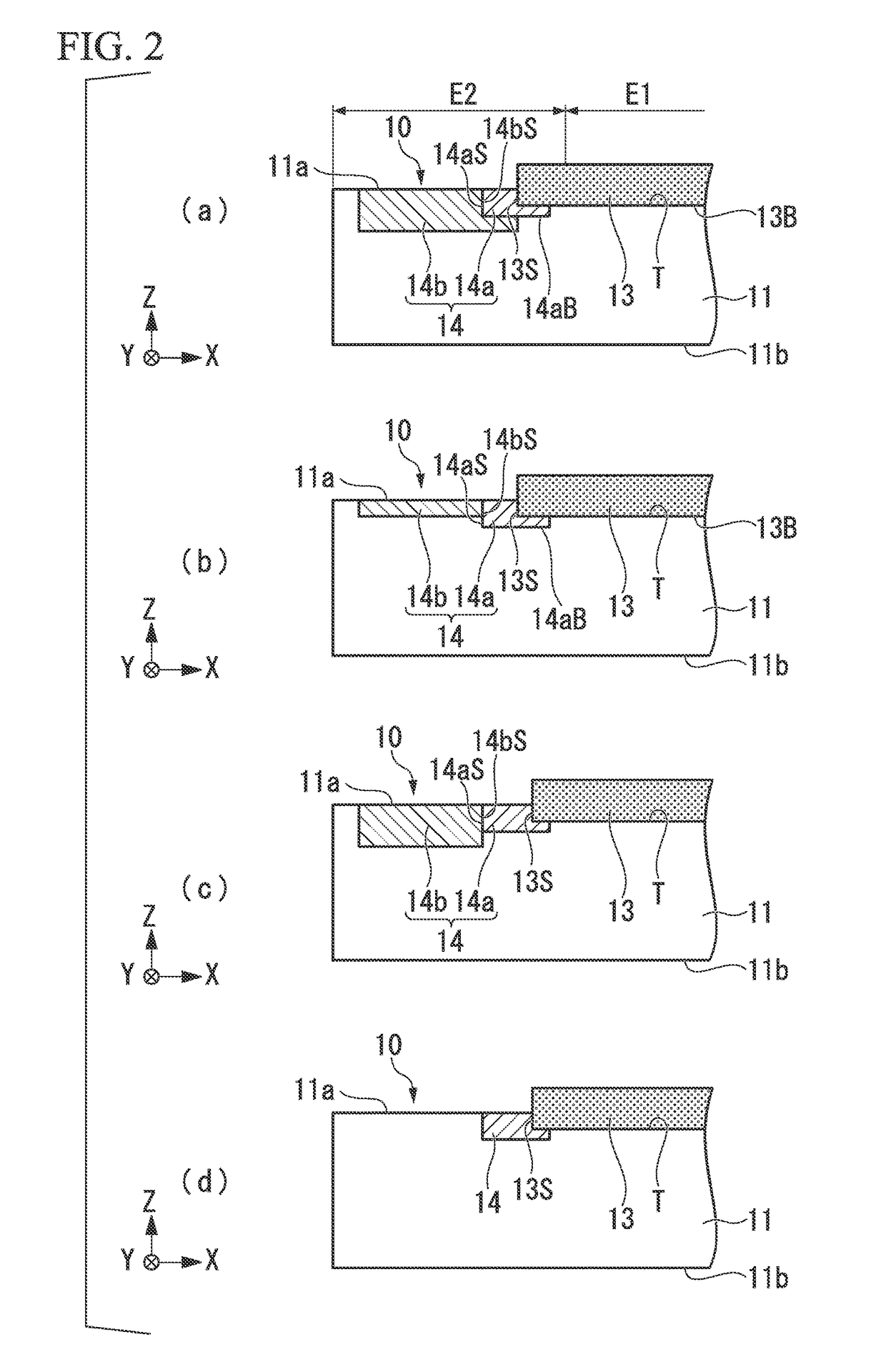
[0057]Modified examples of the above-described Schottky barrier diode of the second embodiment are shown in FIGS. 2(a) to 2(d). Here, similar configurations to those of the second embodiment shown in FIG. 1 are appended with the same numbers, and a description thereof will be omitted.

[0058]In the Schottky barrier diode 10 shown in FIG. 2(a), a part of the side surface 13S of the metal portion 13 and a part of the bottom surface 13B thereof connected to the side surface 13S are in contact with a part of the p+ type semiconductor portion 14a. Then, the p− type semiconductor portion 14b is configured to cover a part of the bottom surface 14aB of the p+ type semiconductor portion 14a from a lower part of the side surface 14bS thereof, and not to be in contact with the metal portion 13.

[0059]In the Schottky barrier diode 10 shown in FIG. 2(b), a part of the side surface 13S of the metal portion 13 and a part of the bottom sur...

third embodiment

(3) Third Embodiment of Schottky Junction

[0062]Next, referring to FIG. 3(a), a Schottky barrier diode according to a third embodiment is described. Here, the same components as those of the above-described Schottky barrier diode according to the second embodiment are appended with the same reference numerals, and a detailed description thereof will be omitted.

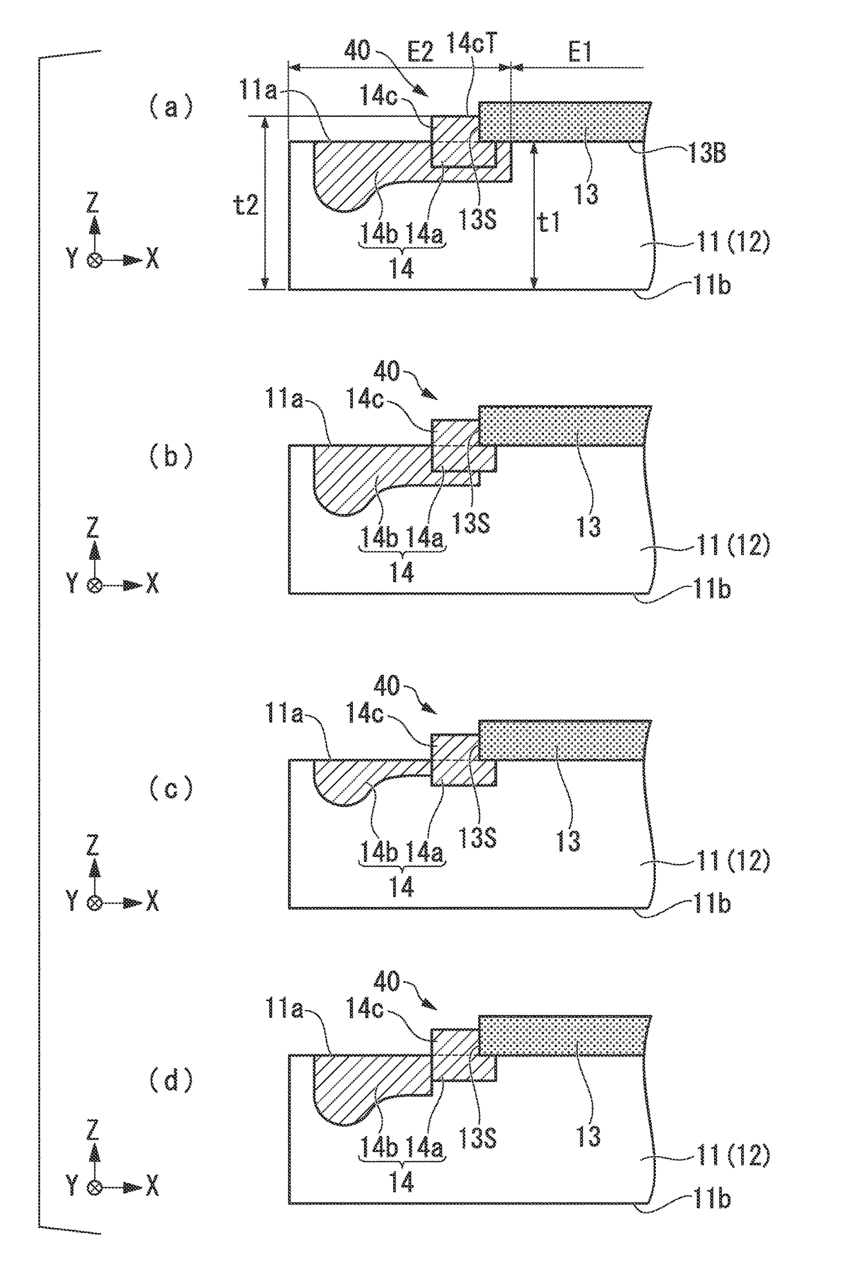
[0063]A Schottky barrier diode 20 shown in FIG. 3(a) has a configuration, a part of which is the same as that of the Schottky barrier diode 20 shown in FIG. 1(a), but which differs therefrom only in a configuration of the p+ type semiconductor portion 14a. A part of the p-type semiconductor portion 14, that is, a p-type semiconductor deposition portion 14c, is formed so as to further extend upward (in the Z-axis direction from the one main surface 11a, which is opposite to the direction toward the other main surface 11b) from the one main surface 11a of the semiconductor substrate 11 where the p-type semiconductor portion 14 is...


PUM


Abstract

It is an objective to improve reverse surge withstand capability of a semiconductor device, for example, a Schottky barrier diode.
A p-type semiconductor section 14 includes a p+ type semiconductor portion (first concentration portion) 14a and a p− type semiconductor portion (second concentration portion) 14b, which have different impurity concentrations from each other. Additionally, a part of a side surface 13S of a metal portion 13 and a part of a bottom surface 13B of the metal portion 13 connected to the side surface 13S thereof are in contact with a part of the p+ type semiconductor portion 14a. Further, at least a part of a side surface 14bS of the p− type semiconductor portion 14b is in contact with a side surface 14aS of the p+ type semiconductor portion 14a.

Description

[0001]This application is the U.S. national phase of International Application No. PCT / JP2013 / 058493 filed 25 Mar. 2013, which designated the U.S., the entire contents of which is hereby incorporated by reference.TECHNICAL FIELD[0002]The present invention relates to a semiconductor device and, more particularly, relates to a technique for improving reverse surge withstand capabilities of diodes.BACKGROUND ART[0003]A diode, which is an example of a semiconductor device, such as a Schottky barrier diode (hereinafter, occasionally referred to as an SBD), is a semiconductor device using rectifying action of a Schottky barrier at a Schottky junction between a semiconductor layer and a metal layer. SBDs can operate at a higher speed than general pn-junction diodes, and have characteristics in that a forward voltage drop is small.[0004]For example, in a switching power supply provided with such an SBD, when emergency stop is performed in an emergency, a reverse voltage applied from the n-t...

Claims


Application Information

Patent Timeline
Patent Type & Authority Patents(United States)
IPC IPC(8): H01L27/095H01L29/06H01L29/872H01L29/36H01L29/16
CPCH01L29/0619H01L29/0615H01L29/0661H01L29/36H01L29/872H01L29/1608
Inventor TOMITA, MASAAKI
Owner SHINDENGEN ELECTRIC MFG CO LTD
Why Eureka
Try Eureka