Charged particle lithography system with alignment sensor and beam measurement sensor

a lithography system and beam measurement technology, applied in photomechanical devices, instruments, nanoinformatics, etc., can solve the problems of not being able to determine the relationship between the substrate to be processed and the charged particle radiation, taking valuable time, and multiple measurements, etc., to achieve the effect of convenient and fast manner

Active Publication Date: 2017-05-30
ASML NETHERLANDS BV
View PDF34 Cites 0 Cited by
  • Summary
  • Abstract
  • Description
  • Claims
  • Application Information

AI Technical Summary

Benefits of technology

[0010]It is an object of the present invention to provide a multi-beamlet charged particle exposure system in which the alignment of a substrate and the radiation used for patterning the substrate can be performed in a relatively easy and fast manner. For this purpose, the present invention provides a multi-beamlet charged particle beamlet lithography system for transferring a pattern to a surface of a substrate. The system comprises a projection system for projecting a plurality of charged particle beamlets onto the surface of the substrate; a chuck moveable with respect to the projection system; a beamlet measurement sensor for determining one or more characteristics of one or more of the charged particle beamlets, the beamlet measurement sensor having a surface for receiving one or more of the charged particle beamlets; and a position mark measurement system for measuring a position of a position mark, the position mark measurement system comprising an alignment sensor. The chuck comprises a substrate support portion for supporting the substrate, a beamlet measurement sensor portion for accommodating the surface of the beamlet measurement sensor, and a position mark portion for accommodating the position mark.
[0019]Together, these two relationships enable calculation of beamlet position relative to the alignment sensor. This is significant due to variations in relative position of the beamlets and the alignment sensor due to effects such as thermal expansion of the structure holding the alignment sensors and final lens elements, drift of the beamlets, etc. The alignment sensor can be used to determine position marks on the substrate, to then enable accurate positioning of the beamlets with respect to the substrate and patterns previously formed on the substrate.

Problems solved by technology

However, it is not possible to determine the relationship between the substrate to be processed and the charged particle radiation, or the projection system used to project such radiation onto the substrate in a direct way.
Consequently, multiple measurements are needed which take valuable time.

Method used


Image

  • Charged particle lithography system with alignment sensor and beam measurement sensor
  • Charged particle lithography system with alignment sensor and beam measurement sensor
  • Charged particle lithography system with alignment sensor and beam measurement sensor

Examples


Embodiment Construction

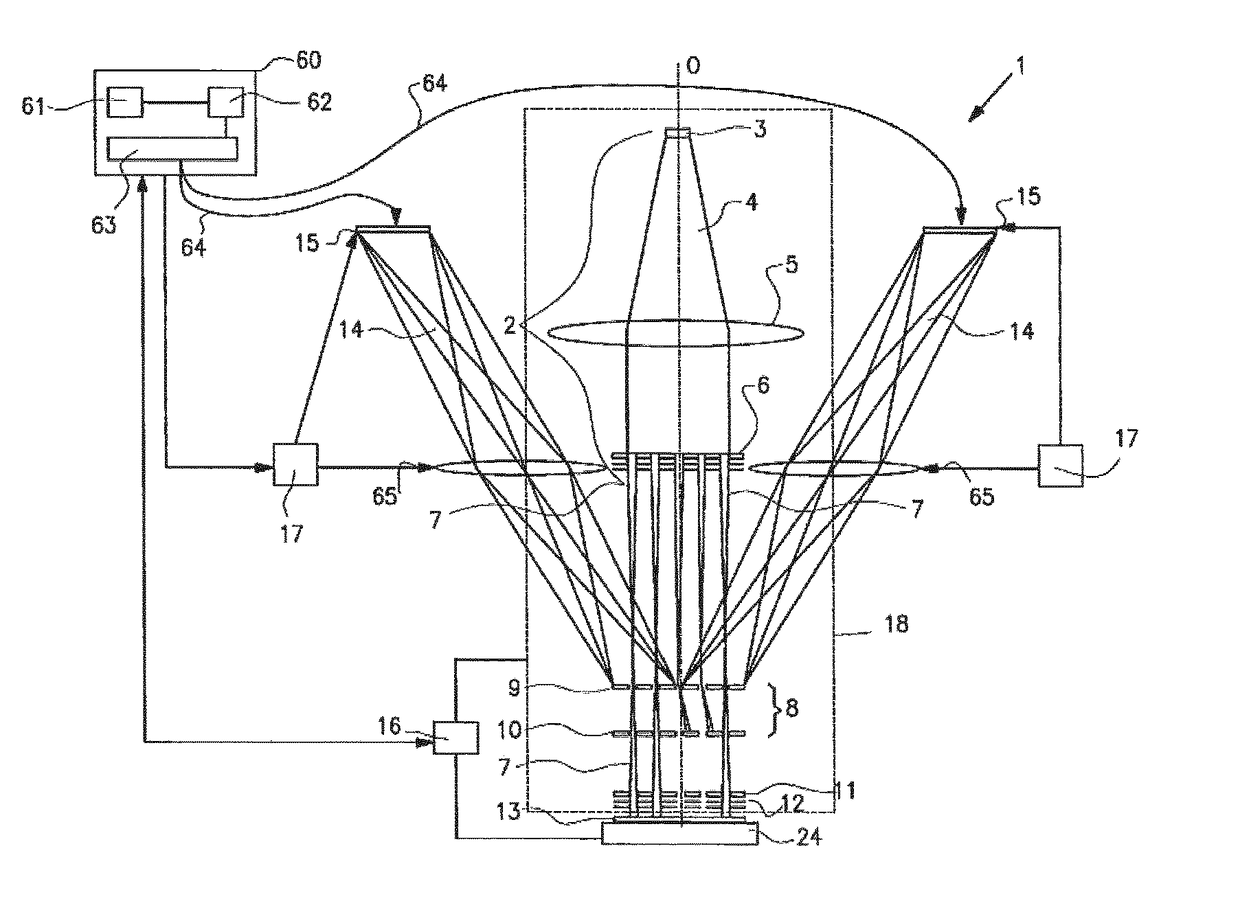
[0045]The following is a description of various embodiments of the invention, given by way of example only and with reference to the figures. The figures are not drawn to scale and merely intended for illustrative purposes.

[0046]FIG. 1 shows a simplified schematic drawing of an embodiment of a charged particle multi-beamlet lithography system 1. Such lithography system is for example described in U.S. Pat. Nos. 6,897,458; 6,958,804; 7,019,908; 7,084,414; 7,129,502; 7,709,815; 7,842,936; 8,089,056 and 8,254,484; U.S. patent application publication nos. 2007 / 0064213; 2009 / 0261267; US 2011 / 0073782; US 2011 / 0079739 and US 2012 / 0091358, which are assigned to the applicant of the present application and which are hereby incorporated by reference in their entirety.

[0047]Such lithography system 1 suitably comprises a beamlet generator generating a plurality of beamlets, a beamlet modulator patterning the beamlets to form modulated beamlets, and a beamlet projector for projecting the modulat...


PUM

PropertyMeasurementUnit
beam energyaaaaaaaaaa
voltageaaaaaaaaaa
diameteraaaaaaaaaa

Abstract

A multi-beamlet charged particle beamlet lithography system for transferring a pattern to a surface of a substrate. The system comprises a projection system (311) for projecting a plurality of charged particle beamlets (7) onto the surface of the substrate; a chuck (313) moveable with respect to the projection system; a beamlet measurement sensor (i.a. 505, 511) for determining one or more characteristics of one or more of the charged particle beamlets, the beamlet measurement sensor having a surface (501) for receiving one or more of the charged particle beamlets; and a position mark measurement system for measuring a position of a position mark (610, 620, 635), the position mark measurement system comprising an alignment sensor (361, 362). The chuck comprises a substrate support portion for supporting the substrate, a beamlet measurement sensor portion (460) for accommodating the surface of the beamlet measurement sensor, and a position mark portion (470) for accommodating the position mark.

Description

BACKGROUND OF THE INVENTION[0001]1. Field of the Invention[0002]The invention relates to a multi-beamlet charged particle lithography system and a method for transferring a pattern to a surface of a substrate, and more particularly relates to a lithography system having an alignment sensor and beam measurement sensor and a method of using the system.[0003]2. Description of the Related Art[0004]In the semiconductor industry, an ever increasing desire exists to manufacture smaller structures with high accuracy and reliability. Charged particle lithography is a promising technology to meet the high demands. In this type of lithography charged particles are manipulated to transfer a onto a target surface of a substrate, typically a wafer.[0005]Lithographic processing generally involves exposure of multiple layers on top of each other so that features formed in subsequent layers may be connected so as to create an integrated circuit. Therefore a pattern to be exposed in a later exposure ...

Claims


Application Information

Patent Timeline
Patent Type & Authority Patents(United States)
IPC IPC(8): H01J37/09H01J37/317B82Y40/00G03F7/20H01J37/304H01J37/16B82Y10/00
CPCG03F7/707B82Y10/00B82Y40/00H01J37/3045H01J37/3177H01J2237/1501H01J2237/1502H01J2237/3045
Inventor SCHEFFERS, PAUL IJMERTMEIJER, JAN ANDRIESSLOT, ERWINKUIPER, VINCENT SYLVESTERVERGEER, NIELS
Owner ASML NETHERLANDS BV
Why Eureka
Try Eureka