
Phase change memory with inter-granular switching

a phase change memory and intergranular switching technology, applied in the field of memory devices, can solve the problems of increasing electrical and mechanical reliability problems, increasing contact area, increasing manufacturing costs, etc., and achieve the effect of reducing increasing the electrical resistance of the conglomerate material

Active Publication Date: 2017-06-06
MACRONIX INT CO LTD
View PDF505 Cites 2 Cited by
  • Summary
  • Abstract
  • Description
  • Claims
  • Application Information

AI Technical Summary

Benefits of technology

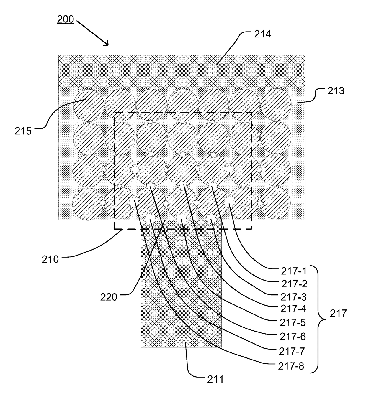
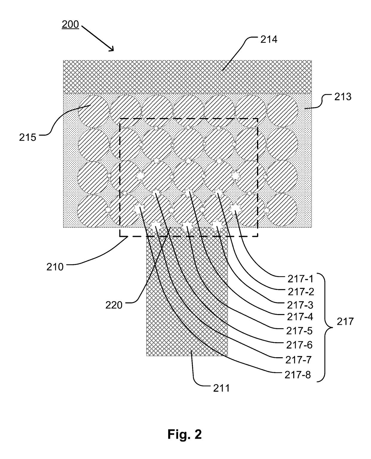
[0010]A memory device having a conglomerate material interposed between a first electrode and a second electrode is described herein. The conglomerate material comprises nanocrystalline grains embedded within an amorphous matrix. The memory device can be operated using inter-granular phase switching. The memory device further comprises circuitry to execute the inter-granular phase switching, wherein the circuitry applies a first bias arrangement to induce formation of amorphous material between the nanocrystalline grains within a region over the first electrode, effective to increase electrical resistance of the conglomerate material between the first and second electrodes above a first threshold without eliminating the nanocrystalline grains in the region, and applies a second bias arrangement to induce expansion of the nanocrystalline grains in the region by an amount effective to decrease electrical resistance of the conglomerate material between the first and second electrodes below a second threshold. The first bias arrangement applied to the memory device is configured to melt the conglomerate material between the nanocrystalline grains and then form the amorphous phase to block the electrical current between the nanocrystalline grains over the first electrode. The second bias arrangement applied to the memory device induces crystallization between the nanocrystalline grains so that the electrical current passes through between the nanocrystalline grains.
[0015]A method for operating a memory device having a conglomerate material between first and second electrodes is also provided. The conglomerate material includes nanocrystalline grains embedded in an amorphous matrix. To store a first data value, the method includes applying a first bias arrangement to induce formation of amorphous material between the nanocrystalline grains within a region over a first electrode, by an amount effective to increase electrical resistance of the conglomerate material between the first and second electrodes above a first threshold without eliminating the nanocrystalline grains in the region. To store a second data value, the method includes applying a second bias arrangement to induce expansion of the nanocrystalline grains within the region by an amount effective to decrease electrical resistance of the conglomerate material between the first and second electrodes below a second threshold.

Problems solved by technology

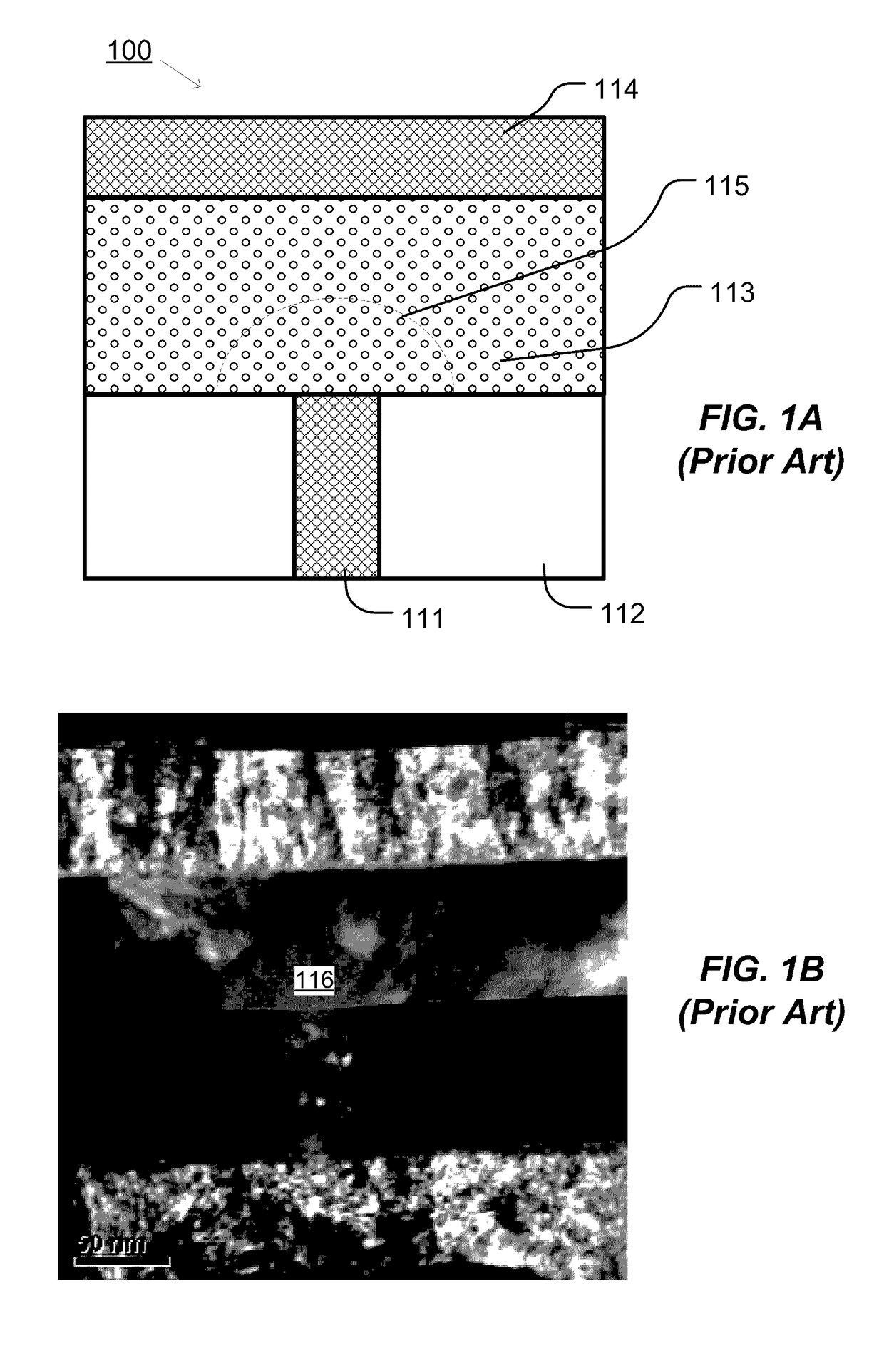
However, forming electrodes of sublithographic feature size involves complicated manufacturing processes, thereby increasing manufacturing costs.
Moreover, the electrical and mechanical reliability issues increase with reducing the contact area.

Method used


Image

  • Phase change memory with inter-granular switching
  • Phase change memory with inter-granular switching
  • Phase change memory with inter-granular switching

Examples


Embodiment Construction

[0039]A detailed description of embodiments of the technology is provided with reference to the FIGS. 2-19.

[0040]FIG. 2 illustrates a memory cell 200 having a conglomerate material including nanocrystalline grains 215 embedded in an amorphous matrix 213. Memory cell 200 includes a first electrode 211 having an electrode surface 220 contacting the conglomerate material, and a second electrode 214 on the conglomerate material. Inter-grain boundaries 217-1, 217-2, . . . and 217-8, collectively indicated 217, are between nanocrystalline grains 215. To simplify the illustration, not all inter-grain boundaries are given their own numeral. The nanocrystalline grains 215 can have a stoichiometry different than the amorphous matrix 213.

[0041]First and second electrodes 211 and 214 may comprise, for example, TiN or TaN. Alternatively, the first and second electrodes 211 and 214 may each be W, WN, TiAlN or TaAlN, or comprise, for further examples, one or more elements selected from the group c...


PUM

PropertyMeasurementUnit
grain sizeaaaaaaaaaa
thicknessaaaaaaaaaa
diameteraaaaaaaaaa

Abstract

A memory device comprising a conglomerate material interposed between a first electrode and a second electrode is provided. The conglomerate material includes nanocrystalline grains embedded in an amorphous matrix. During operations, phase change reactions occur at the inter-grain boundaries in the conglomerate material so as to reduce the operation power.

Description

RELATED APPLICATIONS[0001]This application claims the benefit of U.S. Provisional Patent Application No. 62 / 181,909 filed on 19 Jun. 2015, which application is incorporated by reference as if fully set forth herein.PARTIES TO A JOINT RESEARCH AGREEMENT[0002]International Business Machines Corporation, a New York Corporation, and Macronix International Corporation, Ltd., a Taiwan corporation, are parties to a Joint Research Agreement.BACKGROUND[0003]Technological Field[0004]The present technology relates to memory devices based on phase change materials, and methods for manufacturing and operating such devices.[0005]Description of Related Art[0006]In a phase change memory (PCM), each memory cell includes a phase change memory element. The phase change memory element can be caused to change phase between a crystalline state and an amorphous state. The amorphous state is characterized by higher electrical resistivity than the crystalline state. In operation of the phase change memory e...

Claims


Application Information

Patent Timeline
Patent Type & Authority Patents(United States)
IPC IPC(8): G11C11/16G11C11/15G11C13/00H01L45/00
CPCG11C13/0004G11C13/0069H01L45/06H01L45/1233H01L45/1246H01L45/144H01L45/1625G11C2013/0073H10N70/881H10N70/021G11C2013/0071G11C2013/0078G11C2213/79H10N70/231H10N70/826H10N70/8828H10N70/026H10N70/828
Inventor LUNG, HSIANG-LANHO, YUNG-HAN
Owner MACRONIX INT CO LTD
Learn More