Wirebond structure and method to connect to a microelectronic die

a wire bond and microelectronic die technology, applied in the direction of thin material processing, semiconductor/solid-state device details, semiconductor devices, etc., can solve the problems of disconnection of the bond, weak mechanical strength of the electrical contact formed by connecting the aluminum bond wire directly to the copper pad, and the tendency of the bond to weaken

Inactive Publication Date: 2010-12-21
INTEL CORP
View PDF9 Cites 4 Cited by
  • Summary
  • Abstract
  • Description
  • Claims
  • Application Information

AI Technical Summary

Benefits of technology

[0004]The pads formed in the inter-layer dielectric of the die are typically formed of copper and the bond wires are usually formed from aluminum or gold. Both copper and aluminum, when exposed to an oxidizing environment, such as air, will form a thin layer of oxide on the exposed surfaces. Copper is prone to continues oxidation and aluminum is not. An oxide layer between the aluminum and copper connection will increase the electrical resistance of the conductive path formed by the copper pad and the aluminum bond wire. The strength of the electrical contact formed by connecting the aluminum bond wire directly to the copper pad can also be weak mechanically and deteriorate over time.

Problems solved by technology

The strength of the electrical contact formed by connecting the aluminum bond wire directly to the copper pad can also be weak mechanically and deteriorate over time.
Exposure to high temperatures, such as up to about 200° Celsius or higher, can cause the connection formed between the aluminum bond wire and the copper pad to be unstable resulting in breakage and a disconnection of the bond or resulting in bonds that will be more susceptible to deterioration over time.

Method used


Image

  • Wirebond structure and method to connect to a microelectronic die
  • Wirebond structure and method to connect to a microelectronic die
  • Wirebond structure and method to connect to a microelectronic die

Examples


Embodiment Construction

[0012]In the following detailed description of the preferred embodiments, reference is made to the accompanying drawings which form a part hereof, and in which is shown by way of illustration specific embodiments in which the invention may be practiced. It is to be understood that other embodiments may be utilized and structural changes may be made without departing from the scope of the present invention.

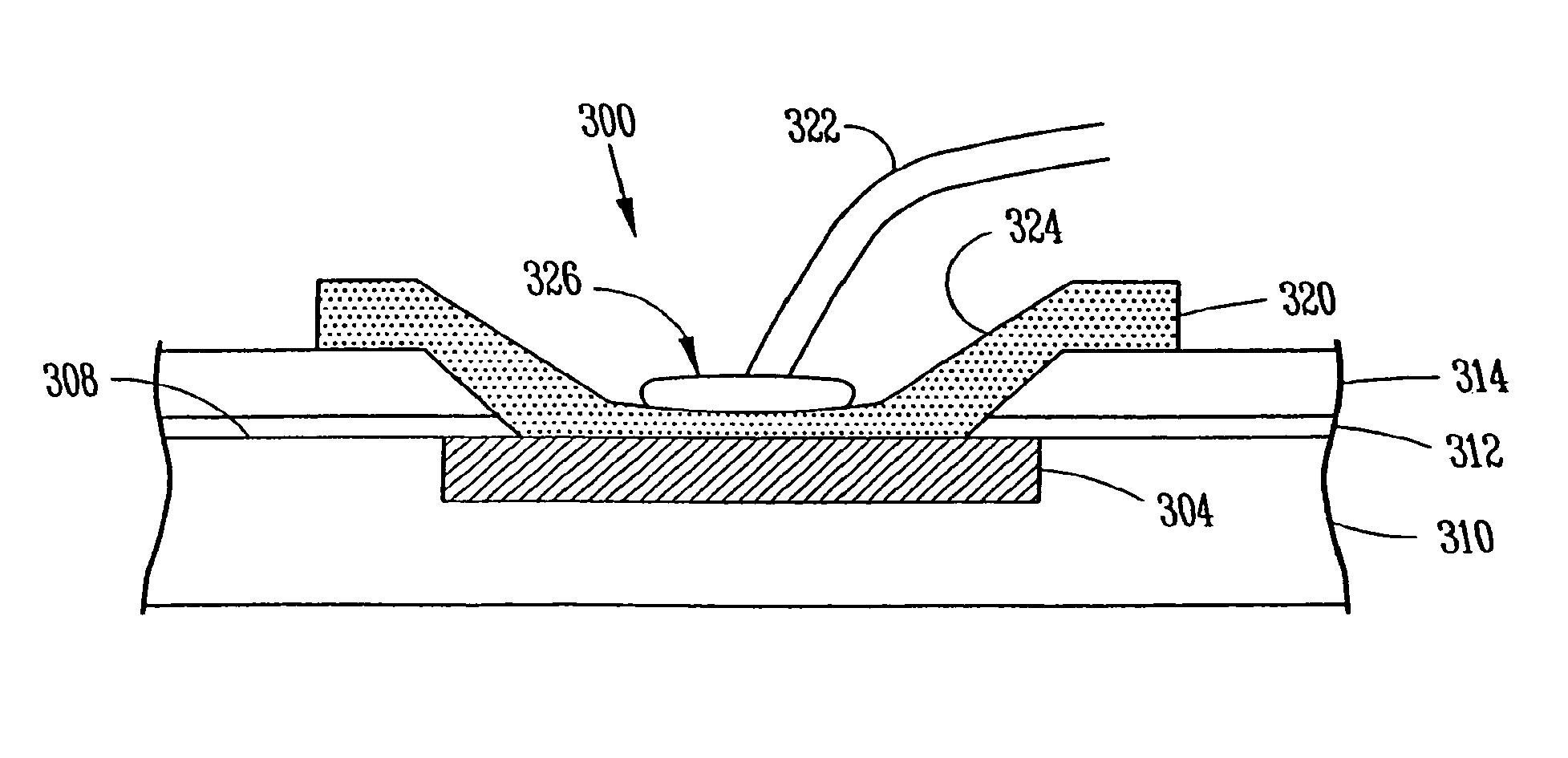
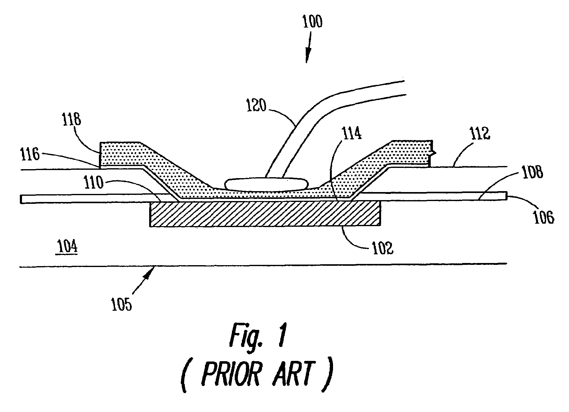
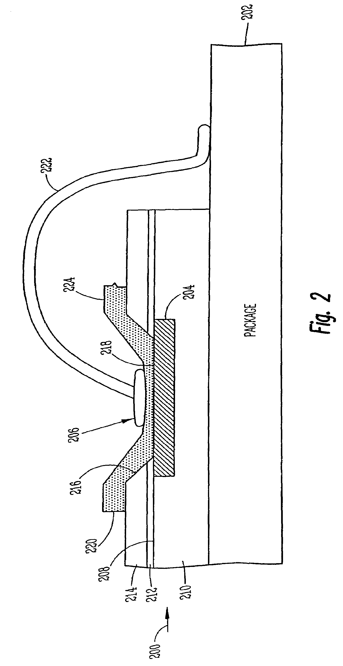
[0013]FIG. 2 is a cross-section of a wirebond structure 206 to connect to a microelectronic die 200 in accordance with the present invention. FIG. 2 shows a partial view of a microelectronic die package 202 connected to the microelectronic die 200 or integrated circuit by the wirebond structure or assembly 206 in accordance with the present invention. The wirebond structure 206 of the microelectronic die 200 includes a copper bond pad 204 that is formed in a surface 208 of an inter-layer dielectric 210 or substrate of the microelectronic die 200. A first passivation layer 212 may b...


PUM

PropertyMeasurementUnit
timeaaaaaaaaaa
annealing temperatureaaaaaaaaaa
temperatureaaaaaaaaaa

Abstract

A wirebond structure includes a copper pad formed on or in a surface of a microelectronic die. A conductive layer is included in contact with the copper pad and a bond wire is bonded to the conductive layer. The conductive layer is formed of a material to provide a stable contact between the bond wire and the copper pad in at least one of an oxidizing environment and an environment with temperatures up to at least about 350° C.

Description

CONTINUATION APPLICATION[0001]This Patent application is a continuation of U.S. patent application Ser. No. 11 / 001,871 filed Dec. 1, 2004, now U.S. Pat. No. 7,393,772 which is a divisional of U.S. patent application Ser. No. 10 / 454,979 filed Jun. 5, 2003, now U.S. Pat. No. 6,924,554 which is a continuation of U.S. patent application Ser. No. 10 / 032,623 filed Oct. 18, 2001, now issued as U.S. Pat. No. 6,683,383, which is incorporated herein by reference.FIELD OF THE INVENTION[0002]The present invention relates generally to microelectronic dice and packaging such devices, and more particularly to a wirebond structure and method to make an electrically connection to a microelectronic die.BACKGROUND INFORMATION[0003]Microelectronic dice, semiconductor chips and the like are typically housed in a protective covering referred to as a package or packaging. Pins formed on the package are electrically connected by bond wires to corresponding pads formed in a substrate or inter-layer dielectr...

Claims


Application Information

Patent Timeline
Patent Type & Authority Patents(United States)
IPC IPC(8): H01L21/50H01L21/48H01L21/44H01L21/461H01L21/603H01L23/485
CPCH01L24/03H01L24/05H01L24/48H01L24/85H01L24/45H01L2224/04042H01L2224/05009H01L2224/05073H01L2224/05147H01L2224/05644H01L2224/05647H01L2224/05664H01L2224/05666H01L2224/05669H01L2224/45124H01L2224/45144H01L2224/48091H01L2224/48227H01L2224/48465H01L2224/85H01L2924/01005H01L2924/01006H01L2924/01013H01L2924/01014H01L2924/01022H01L2924/01029H01L2924/01033H01L2924/01046H01L2924/01073H01L2924/01078H01L2924/01079H01L2924/05042H01L2924/14H01L2924/00014H01L2224/48644H01L2224/48647H01L2224/48664H01L2224/48666H01L2224/48669H01L2224/48747H01L2224/48764H01L2224/48766H01L2224/48769H01L2224/05556Y10T428/24248Y10T428/1291H01L2224/78H01L2924/00H01L2224/48744H01L2224/85205H01L2224/02126
Inventor GLEIXNER, ROBERT J.DANIELSON, DONALDPALUDA, PATRICK M.NAIK, RAJAN
Owner INTEL CORP
Why Eureka
Try Eureka