

Integrated circuit packaging system with plated copper posts and method of manufacture thereof
a technology of integrated circuit and packaging system, which is applied in the direction of printed circuit manufacturing, printed circuit non-printed electric component association, printed element electric connection formation, etc., can solve the problems of long time-consuming, long-standing, and long-standing eluded skilled in the art solutions to these problems
- Summary
- Abstract
- Description
- Claims
- Application Information
AI Technical Summary
Benefits of technology
Problems solved by technology
Method used
Image

Examples
first embodiment
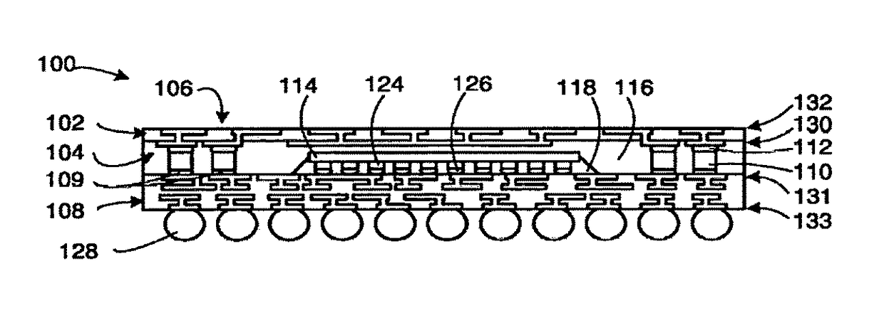
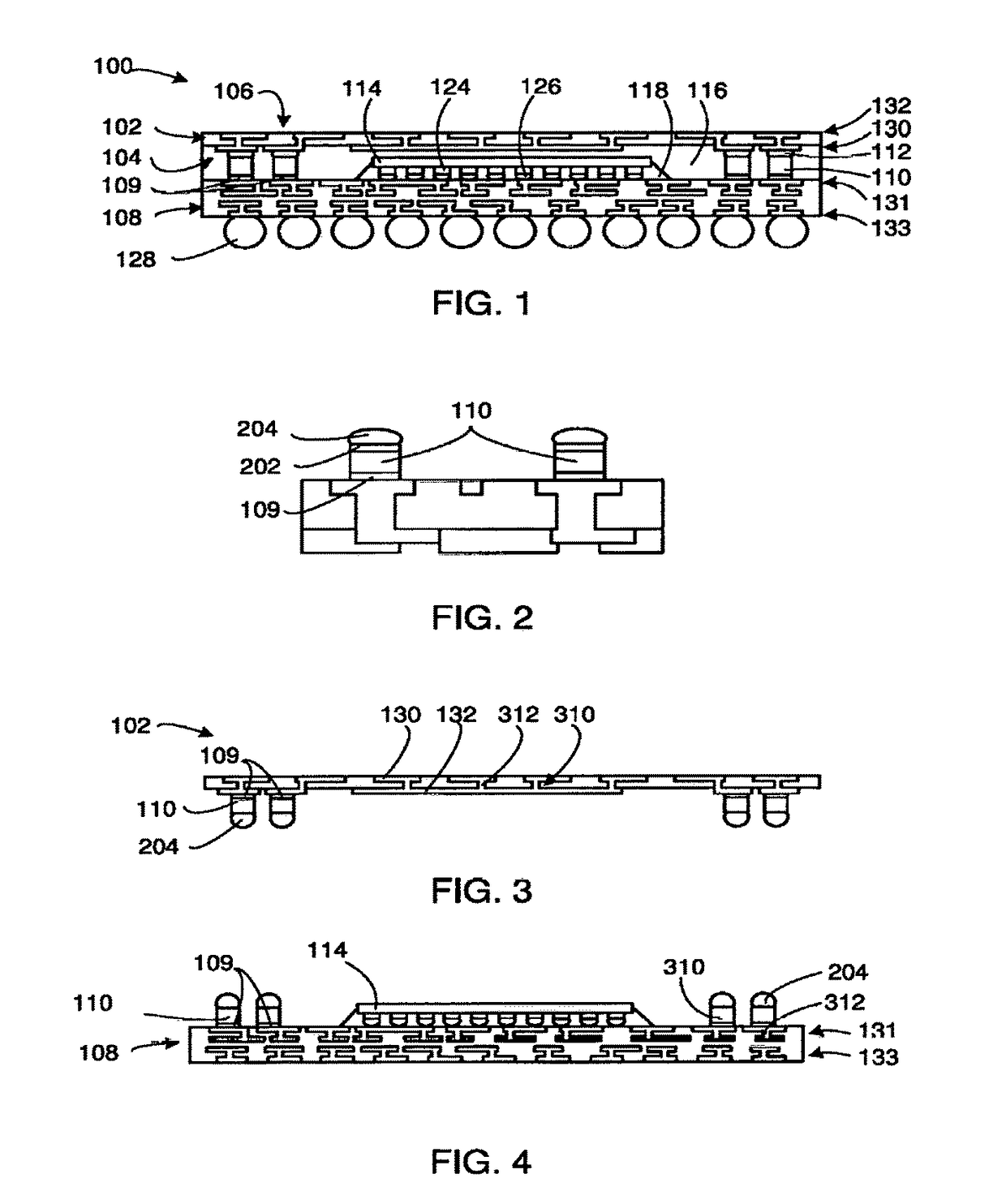
[0050]Referring now to FIG. 1, therein is shown a side view of an integrated circuit packaging system 100 in the present invention. The integrated circuit packaging system 100 can include an interposer 102 mounted over a substrate 108 with an integrated circuit 114 mounted on the substrate 108.
[0051]The interposer 102 is a structural element for redistributing electrical signals. For example the interposer 102 can be a redistribution layer, a carrier, a circuit board, an adapter, or a combination thereof.
[0052]The substrate 108 is a structural element for redistributing electrical signals from an active device. For example, the substrate 108 can be a redistribution layer, a chip carrier, a circuit board, or a combination thereof.
[0053]The interposer 102 can be mounted over the substrate 108. The interposer 102 and the substrate 108 can be electrically connected with a copper film 109 and copper posts 110 between the interposer and the substrate 108. The copper posts 110 are electric...
second embodiment
[0174]Referring now to FIG. 24, therein is shown a side view of an integrated circuit packaging system in a The integrated circuit packaging system 2400 can include the interposer 2302 having the copper posts 2310 tipped with the solder pads 2312 mounted on the substrate 2308. An encapsulation 2416 can be between the interposer 2302 and the substrate 2308.
[0175]It has been discovered that forming the copper posts 2310 on the interposer 2302 improves packaging density by reducing the package height. The formation of the copper posts 2310 on the interposer 2302 provides improved control of package size and the separation between the interposer 2302 and the substrate 2308.
[0176]Referring now to FIG. 25, therein is shown a side view of a substrate with copper posts 2510 and the solder pads 2512. The substrate 2508 can include the copper posts 2510 formed directly on the substrate 2508. The copper posts 2510 can include the solder pads 2512 on the ends of the copper posts 2510. The inte...
third embodiment
[0177]Referring now to FIG. 26, therein is shown a side view of an integrated circuit packaging system in a The integrated circuit packaging system 2600 can include the substrate 2508 having the copper posts 2510 tipped with the solder pads 2512. The interposer 2502 can be mounted directly on the solder pads 2512 of the copper posts 2510 of the substrate 2508. An encapsulation 2616 can be between the interposer 2502 and the substrate 2508.
[0178]It has been discovered that forming the copper posts 2510 on the substrate 2508 improves packaging density by reducing the package height. The formation of the copper posts 2510 on the substrate 2508 provides improved control of package size and the separation between the interposer 2502 and the substrate 2508.
[0179]Referring now to FIG. 27, therein is shown a side view of a substrate with solder pads. The interposer 2702 can include the copper posts 2710 formed directly on the interposer 2702. The substrate 2708 can include the solder pads ...
PUM
 Abstract
Description
Claims
Application Information