Semiconductor device

a semiconductor and semiconductor technology, applied in semiconductor devices, electrical equipment, instruments, etc., can solve the problems of small power consumption of display devices to which a transistor including an oxide semiconductor is applied, and achieve the effects of low leakage current, excellent electrical characteristics, and high reliability

Active Publication Date: 2017-07-11
SEMICON ENERGY LAB CO LTD
View PDF158 Cites 9 Cited by
  • Summary
  • Abstract
  • Description
  • Claims
  • Application Information

AI Technical Summary

Benefits of technology

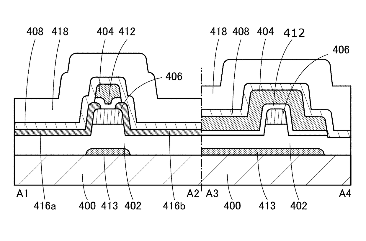
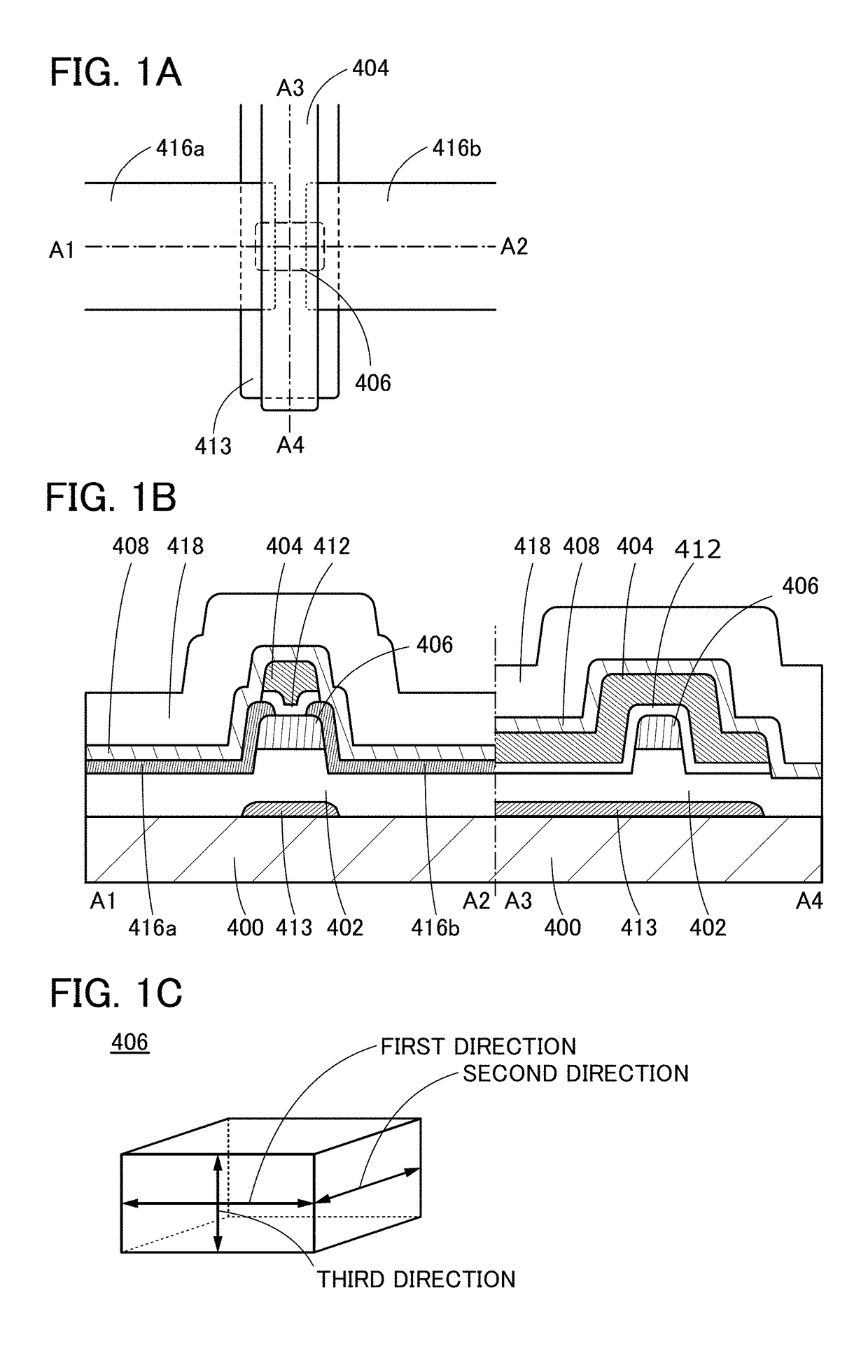
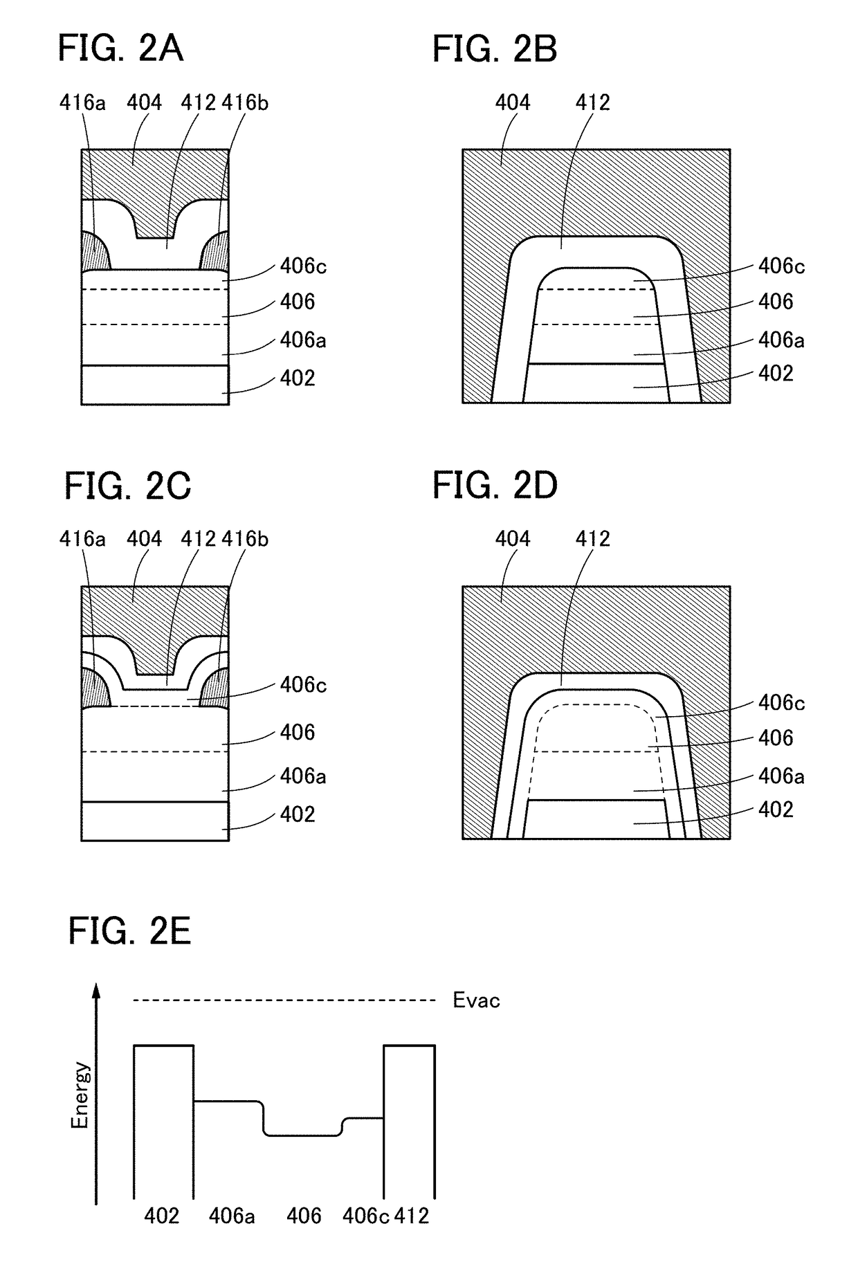
[0018]One object of embodiments of the present invention is to provide a transistor whose channel is formed in a semiconductor having dielectric anisotropy. Another object is to provide a transistor having a small subthreshold swing value. Another object is to provide a transistor having a small short-channel effect. Another object is to provide a transistor having normally-off electrical characteristics. Another object is to provide a transistor having a low leakage current in an off state. Another object is to provide a transistor having excellent electrical characteristics. Another object is to provide a transistor having high reliability. Another object is to provide a transistor having high frequency characteristics.
[0027]A transistor whose channel is formed in a semiconductor having dielectric anisotropy can be provided. A transistor having a small subthreshold swing value can be provided. A transistor having a small short-channel effect can be provided. A transistor having normally-off electrical characteristics can be provided. A transistor having a low leakage current in an off state can be provided. A transistor having excellent electrical characteristics can be provided. A transistor having high reliability can be provided. A transistor having high frequency characteristics can be provided.

Problems solved by technology

For example, a display device to which a transistor including an oxide semiconductor is applied is known to have small power consumption.

Method used


Image

  • Semiconductor device
  • Semiconductor device
  • Semiconductor device

Examples


example 1

[0381]In this example, dielectric constants of oxide semiconductors were evaluated by the density functional perturbation theory.

[0382]The following oxide semiconductors were calculated: zinc oxide, an In—Ga—Zn oxide with an atomic ratio In:Ga:Zn of 1:1:1, and an In—Ga—Zn oxide with an atomic ratio In:Ga:Zn of 3:1:2. The structure of zinc oxide used in the calculation included 4 atoms and the structures of the In—Ga—Zn oxides used in the calculation included 28 atoms.

[0383]Zinc oxide with a wurtzite type structure was assumed (see FIG. 32A). As the In—Ga—Zn oxide with an atomic ratio In:Ga:Zn of 1:1:1, InGaO3(ZnO)m having a homologous structure where m was 1 was assumed (see FIG. 32B). As the In—Ga—Zn oxide with an atomic ratio In:Ga:Zn of 3:1:2, the same structure as that of the In—Ga—Zn oxide with an atomic ratio In:Ga:Zn of 1:1:1 was assumed and the composition was adjusted by substituting In for Ga of the Ga—Zn—O layer. Thus, depending on the position where In is substituted for...

example 2

[0391]In this example, a relation between the dielectric constant of a channel formation region and electrical characteristics of the transistor was evaluated by calculation.

[0392]FIGS. 34A to 34C are cross-sectional views of a transistor having a three-dimensional structure which was subjected to electrical characteristic calculation. FIG. 34A is a cross-sectional view in the channel length direction. FIG. 34B is a cross-sectional view taken along dashed-dotted line B in FIG. 34A. FIG. 34C is a cross-sectional view taken along dashed-dotted line C in FIG. 34A.

[0393]As illustrated in FIG. 34A, the transistor includes a first insulator (represented by BI), a first semiconductor (represented by S1) over BI, a second semiconductor (represented by S2) over S1, a first conductor and a second conductor (both represented by ME) over S2, a third semiconductor (represented by S3) over S2 and ME, a second insulator (represented by GI) over S3, and a third conductor (represented by GE) over GI...


PUM

PropertyMeasurementUnit
angleaaaaaaaaaa
angleaaaaaaaaaa
angleaaaaaaaaaa

Abstract

A transistor whose channel is formed in a semiconductor having dielectric anisotropy is provided. A transistor having a small subthreshold swing value is provided. A transistor having normally-off electrical characteristics is provided. A transistor having a low leakage current in an off state is provided. A semiconductor device includes an insulator, a semiconductor, and a conductor. In the semiconductor device, the semiconductor includes a region overlapping with the conductor with the insulator positioned therebetween, and a dielectric constant of the region in a direction perpendicular to a top surface of the region is higher than a dielectric constant of the region in a direction parallel to the top surface.

Description

BACKGROUND OF THE INVENTION[0001]1. Field of the Invention[0002]The present invention relates to, for example, a semiconductor, a transistor, and a semiconductor device. The present invention relates to, for example, a method for manufacturing a semiconductor, a transistor, and a semiconductor device. The present invention relates to, for example, a semiconductor, a display device, a light-emitting device, a lighting device, a power storage device, a memory device, a processor, and an electronic device. The present invention relates to a method for manufacturing a semiconductor, a display device, a liquid crystal display device, a light-emitting device, a memory device, and an electronic device. The present invention relates to a driving method of a semiconductor device, a display device, a liquid crystal display device, a light-emitting device, a memory device, and an electronic device.[0003]Note that one embodiment of the present invention is not limited to the above technical fie...

Claims


Application Information

Patent Timeline
Patent Type & Authority Patents(United States)
IPC IPC(8): H01L29/78H01L29/786H01L29/04H01L27/06G02F1/1368H01L21/822
CPCH01L29/7869G02F1/1368H01L21/8221H01L27/0688H01L29/045H01L29/78696G02F2201/58H01L29/78648H01L27/1225
Inventor KOBAYASHI, YOSHIYUKIMATSUDA, SHINPEIMATSUBAYASHI, DAISUKETOMISU, HIROYUKI
Owner SEMICON ENERGY LAB CO LTD
Why Eureka
Try Eureka