Magneto-resistive devices including a free layer having different magnetic properties during operations

a free layer and magnetic resistance technology, applied in the field of magnetoresistive devices, can solve the problems of low perpendicular magnetic anisotropy, increase in the thickness of the device, increase in the magnetic switching current and power consumption, etc., and achieve the effect of stably preserving the information stored therein, low power consumption, and high data retention property

Active Publication Date: 2017-07-25
SAMSUNG ELECTRONICS CO LTD
View PDF41 Cites 6 Cited by
  • Summary
  • Abstract
  • Description
  • Claims
  • Application Information

AI Technical Summary

Benefits of technology

[0014]Data-storage media, such as a magneto-resistive memory device, are needed to have a low power consumption property and a high data retention property (i.e., to stably preserve information stored therein). Heat generated in the data-storage media itself or in other devices may be applied to the data-storage media, and thus, it is necessary for a data-storing layer or a free layer of the magneto-resistive device to have high magnetization thermal stability. However, for the magneto-resistive device described in Patent Document 1, it is possible to realize a low power consumption property, but any method for achieving high magnetic stability is not described in Patent Document 1.
[0015]Aspects of the present disclosure are to address at least the above-mentioned problems and / or disadvantages and to provide at least a magneto-resistive device with a low power consumption property and improved stability.

Problems solved by technology

However, for CoFeB-based materials, since the perpendicular magnetic anisotropy is realized using an interface magnetic anisotropy, the use of the CoFeB-based materials may lead to a low perpendicular magnetic anisotropy.
However, this may lead to an increase in layer thickness of a device and consequently an increase in magnetization switching current and power consumption.

Method used


Image

  • Magneto-resistive devices including a free layer having different magnetic properties during operations
  • Magneto-resistive devices including a free layer having different magnetic properties during operations
  • Magneto-resistive devices including a free layer having different magnetic properties during operations

Examples


Embodiment Construction

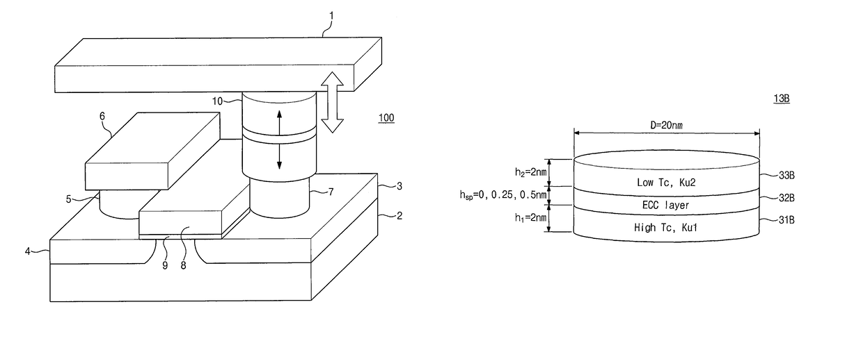
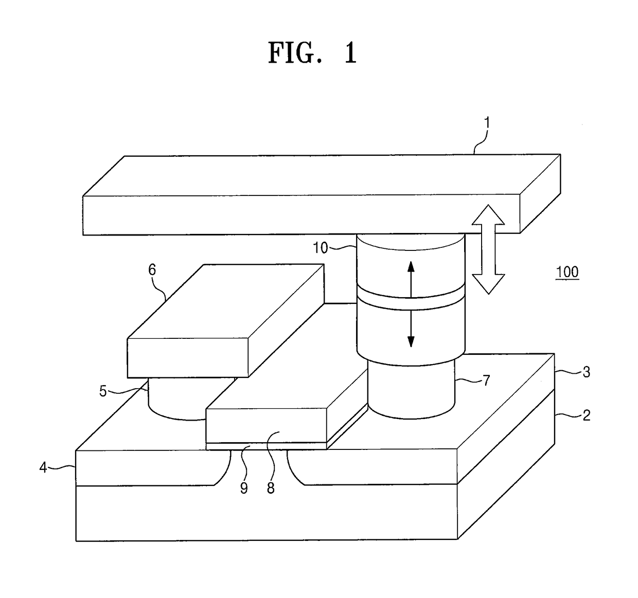
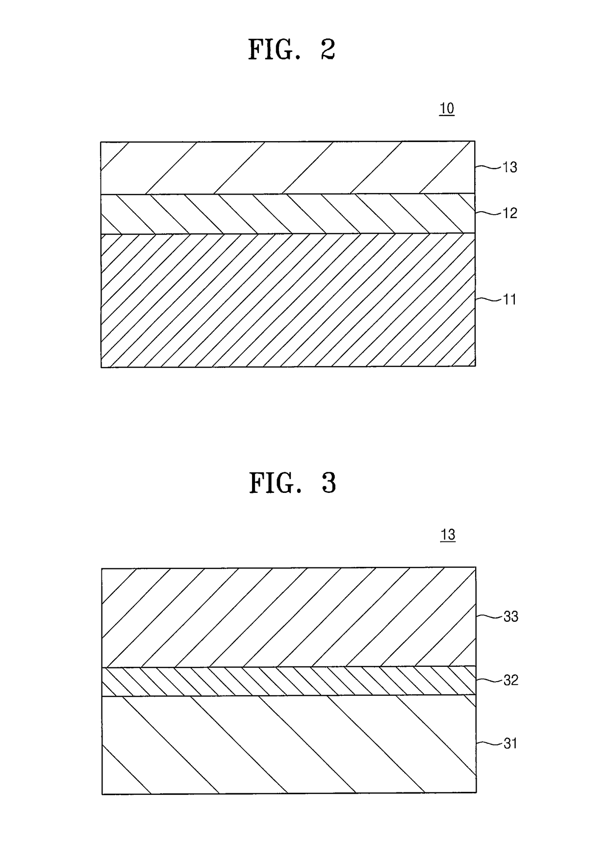
[0057]Example embodiments of the inventive concepts will now be described more fully with reference to the accompanying drawings, in which example embodiments are shown. Example embodiments of the inventive concepts may, however, be embodied in many different forms and should not be construed as being limited to the embodiments set forth herein; rather, these embodiments are provided so that this disclosure will be thorough and complete, and will fully convey the concepts of example embodiments to those of ordinary skill in the art. In the drawings, the thicknesses of layers and regions may be exaggerated for clarity.

[0058]It will be understood that when an element is referred to as being “connected” or “coupled” to another element, it can be directly connected or coupled to the other element or intervening elements may be present. In contrast, when an element is referred to as being “directly connected” or “directly coupled” to another element, there are no intervening elements pre...


PUM

PropertyMeasurementUnit
Curie temperatureaaaaaaaaaa
thicknessaaaaaaaaaa
Curie temperatureaaaaaaaaaa

Abstract

Magneto-resistive devices with lower power consumption and higher stability are provided. The magneto-resistive devices may include a pinned layer, a free layer and an insulating layer between the pinned layer and the free layer. The pinned layer, the free layer and the insulating layer may constitute a magnetic tunnel junction. The free layer may include a first magnetic layer and a second magnetic layer that has a Curie temperature lower than a Curie temperature of the first magnetic layer.

Description

CROSS-REFERENCE TO RELATED APPLICATIONS[0001]This U.S. non-provisional patent application claims priority under 35 U.S.C. §119 to Japanese Patent Application No. 2014-221404, filed on Oct. 30, 2014, in the Japan Patent Office, and Korean Patent Application No. 10-2015-0043084, filed on Mar. 27, 2015, in the Korean Intellectual Property Office, the disclosures of which are hereby incorporated by reference in their entireties.BACKGROUND OF THE INVENTION[0002]Example embodiments of the inventive concepts generally relate to a magneto-resistive device including magnetic tunnel junctions, and in particular, to a magnetic tunnel device using a spin transfer magnetization inversion technique and a magneto-resistive device of a magneto-resistive random access memory (MRAM).[0003]A magneto-resistive random access memory (MRAM) is an emerging nonvolatile memory device with excellent properties, such as high speed, low power consumption, and large capacity. In the magneto-resistive memory, a m...

Claims


Application Information

Patent Timeline
Patent Type & Authority Patents(United States)
IPC IPC(8): G11B5/39G11C11/16H01L43/08H01L43/10H01L43/02H01L27/22
CPCG11C11/161G11B5/3906G11B5/3909G11C11/1673G11C11/1675H01L43/02H01L43/08H01L43/10H01L27/228H10B61/22H10N50/85H10N50/10H10N50/80
Inventor KITA, EIJISONOBE, YOSHIAKI
Owner SAMSUNG ELECTRONICS CO LTD
Why Eureka
Try Eureka