Thin Film Transistor Substrate and Display Using the Same

a thin film transistor and substrate technology, applied in the direction of basic electric elements, electrical equipment, semiconductor devices, etc., can solve the problem of difficult to implement portable/wearable devices with low power consumption as desired, and achieve the effect of simplifying the manufacturing process

Active Publication Date: 2017-03-02
LG DISPLAY CO LTD
View PDF4 Cites 8 Cited by
  • Summary
  • Abstract
  • Description
  • Claims
  • Application Information

AI Technical Summary

Benefits of technology

[0011]Another advantage of the present disclosure is to provide a method of manufacturing a thin film transistor substrate having two different types of transistors for a flat panel display by a simplified manufacturing process.
[0020]The thin film transistor substrate and a flat panel display adopting the same substrate according to the present disclosure comprises two different type thin film transistors on the same substrate, so that the demerit of any one type thin film transistor can be compensated by the other type thin film transistor. Especially, including the thin film transistor having the low off-current characteristics, the display can be driven with the low frequency, it can have the low power consumption property and it can be applied to the portable and / or wearable appliances. Further, the thin film transistor substrate according to the present disclosure includes a passivation layer having the oxide material at the lower layer and the nitride material at the upper layer. With this structure of the passivation layer, the thin film transistor substrate can have storage capacitor ensuring the maximum capacitance with the minimum area, as well as the oxide semiconductor material can be protected from the hydrogen materials.

Problems solved by technology

However, with the current display technology, it may be difficult to implement a portable / wearable device with low power consumption as desired.

Method used


Image

  • Thin Film Transistor Substrate and Display Using the Same
  • Thin Film Transistor Substrate and Display Using the Same
  • Thin Film Transistor Substrate and Display Using the Same

Examples


first embodiment

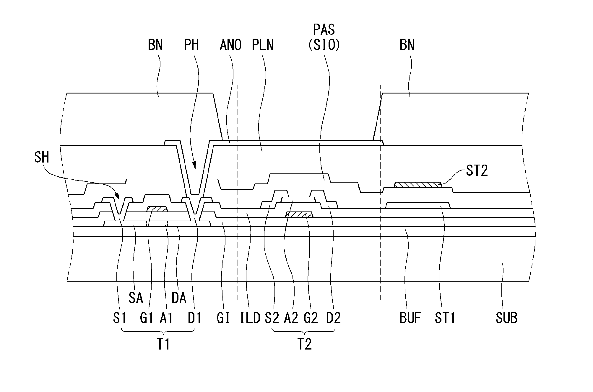
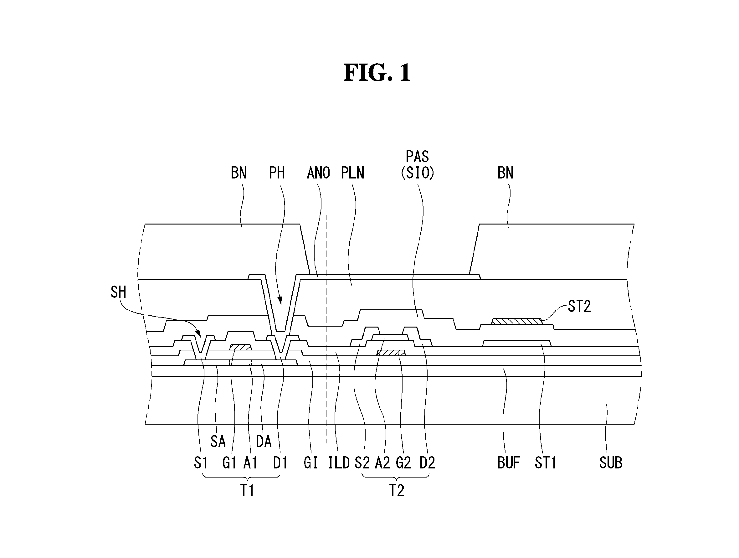
[0036]Referring to FIG. 1, we will explain about the first embodiment of the present disclosure. FIG. 1 is a cross sectional view illustrating a structure of a thin film transistor substrate for a flat panel display in which two different type thin film transistors are formed, according to the first embodiment of the present disclosure. Here, we will explain with the cross sectional views mainly because it clearly shows the main features of the present disclosure, in convenience, the plan view is not used.

[0037]Referring to FIG. 1, the thin film transistor substrate for a flat panel display according to the first embodiment comprises a first thin film transistor T1 and a second thin film transistor T2 which are disposed on the same substrate SUB. The first and second thin film transistors T1 and T2 may be disposed apart from each other, or they may be disposed within a relatively close distance. Otherwise these two thin film transistors are disposed as being overlapped each other.

[0...

second embodiment

[0072]Hereinafter, referring to FIG. 3, we will explain about the second embodiment of the present disclosure. FIG. 3 is a cross sectional view illustrating a structure of a thin film transistor substrate for a flat panel display in which two different type thin film transistors are formed, according to the second embodiment of the present disclosure.

[0073]In the first embodiment, for forming the storage capacitance, the first storage capacitor electrode ST1 and the second storage capacitor electrode ST2 are overlapped with a passivation layer PAS including the oxide layer SIO there-between. In order to ensure the surface property and uniformity, the oxide layer SIO should have a thickness of at least 3000A. Therefore, the storage capacitance is formed at the oxide layer SIO having the thickness of at least 3,000 Å interposed between the first storage capacitor electrode ST1 and the second storage capacitor electrode ST2.

[0074]The oxide layer SIO has a lower dielectric constant (or ...


PUM


Abstract

A display is disclosed which includes a substrate, a first thin film transistor, a second thin film transistor, a first storage capacitor electrode, an oxide layer, a nitride layer, a second storage capacitor electrode, a planar layer and a pixel electrode. The first thin film transistor is disposed in a first area on the substrate. The second thin film transistor is disposed in a second area on the substrate. The first storage capacitor electrode is disposed in a third area on the substrate. The oxide layer covers the first thin film transistor and the second thin film transistor, and exposes the first storage capacitor electrode. The nitride layer is disposed on the oxide layer and covers the first storage capacitor electrode. The second storage capacitor electrode includes a first metal layer and a second metal layer, and overlaps with the first storage capacitor electrode on the nitride layer. The planar layer covers the first thin film transistor, the second thin film transistor and the second storage capacitor electrode. The pixel electrode is disposed on the planar layer.

Description

[0001]This application claims priority from and the benefit under 35 U.S.C. §119(a) of Korea Patent Application No. 10-2015-0120902 filed on Aug. 27, 2015, which is incorporated herein by reference for all purposes as if fully set forth herein.BACKGROUND OF THE INVENTION[0002]Field of the Invention[0003]The present disclosure relates to a thin film transistor substrate, a display including the same and a method of manufacturing the same.[0004]Discussion of the Related Art[0005]Nowadays, as the information society is developed, the requirements of displays for representing information are increasing. Accordingly, various flat panel displays (or ‘FPD’) are developed for overcoming many drawbacks of the cathode ray tube (or ‘CRT’) which is heavy and bulky. The flat panel display devices include a liquid crystal display device (or ‘LCD’), a plasma display panel (or ‘PDP’), an organic light emitting display device (or ‘OLED’) and an electrophoresis display device (or ‘ED’).[0006]The disp...

Claims


Application Information

Patent Timeline
Patent Type & Authority Applications(United States)
IPC IPC(8): H01L27/12
CPCH01L27/1255H01L27/124H01L27/1225H01L27/1251H01L27/1288H01L27/1248H01L27/1285H01L27/1259
Inventor NOH, SOYOUNG
Owner LG DISPLAY CO LTD
Why Eureka
Try Eureka