Method for manufacturing electronic device

a manufacturing method and electronic technology, applied in the direction of semiconductor/solid-state device details, chemical vapor deposition coating, coating, etc., can solve the problems of less easily permeable solution, difficult etching and liftoff, exposed terminals on the substrate, etc., to achieve high manufacturing productivity, simple step, and accurate removal of only the coating film

Inactive Publication Date: 2017-08-01
PIONEER CORP +1
View PDF15 Cites 0 Cited by
  • Summary
  • Abstract
  • Description
  • Claims
  • Application Information

AI Technical Summary

Benefits of technology

[0008]The present invention has an example of an object in dealing with such problems. That is, it is an object of the present invention to, for example, in forming, with the ALD film forming method or the like, a coating film on a substrate on which an element is formed, make it possible to remove the coating film on a connection terminal area with a simple step; make is possible to obtain high productivity in manufacturing of an electronic device for forming the coating film on the substrate, and make it possible to accurately remove only the coating film on the connection terminal area to prevent an element forming area from being adversely affected.

Problems solved by technology

A solution less easily permeates because of high moisture barrier properties of the coating film.
Etching and liftoff are difficult.
Therefore, it is a problem how a connection terminal on the substrate is exposed after the film formation.
However, with this method, there is a problem in that a step of sticking the mask tape is complicated and satisfactory productivity is not obtained.
Therefore, in a sticking step for the mask tape, it is difficult to accurately stick the mask tape and high productivity cannot be realized.
When the connection terminal area and the element forming area are close to each other, there is a concern that sealing performance of the element is deteriorated because the film around the mask tape peels.

Method used


Image

  • Method for manufacturing electronic device
  • Method for manufacturing electronic device
  • Method for manufacturing electronic device

Examples


Embodiment Construction

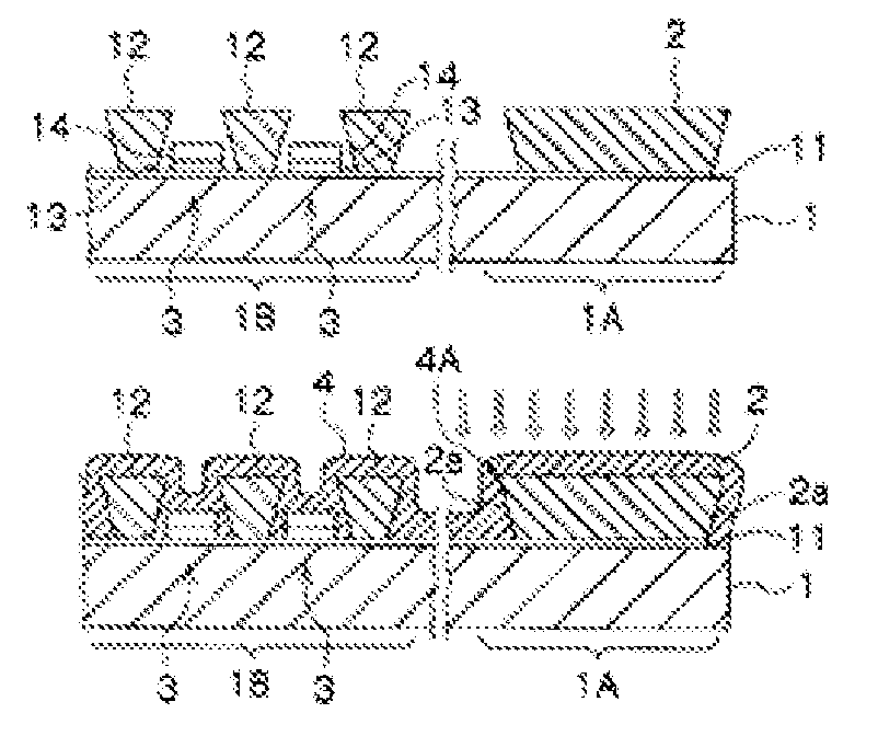
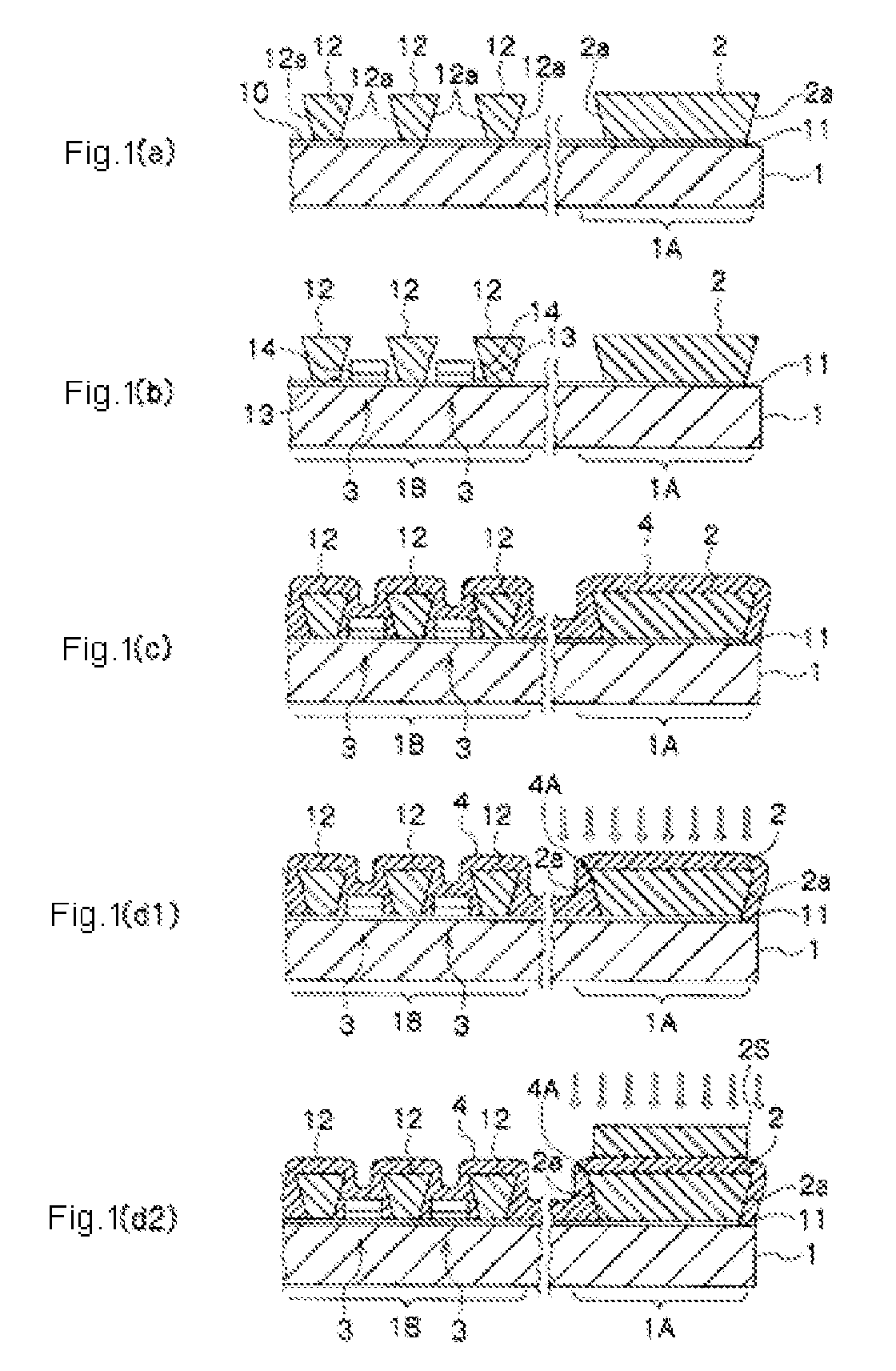
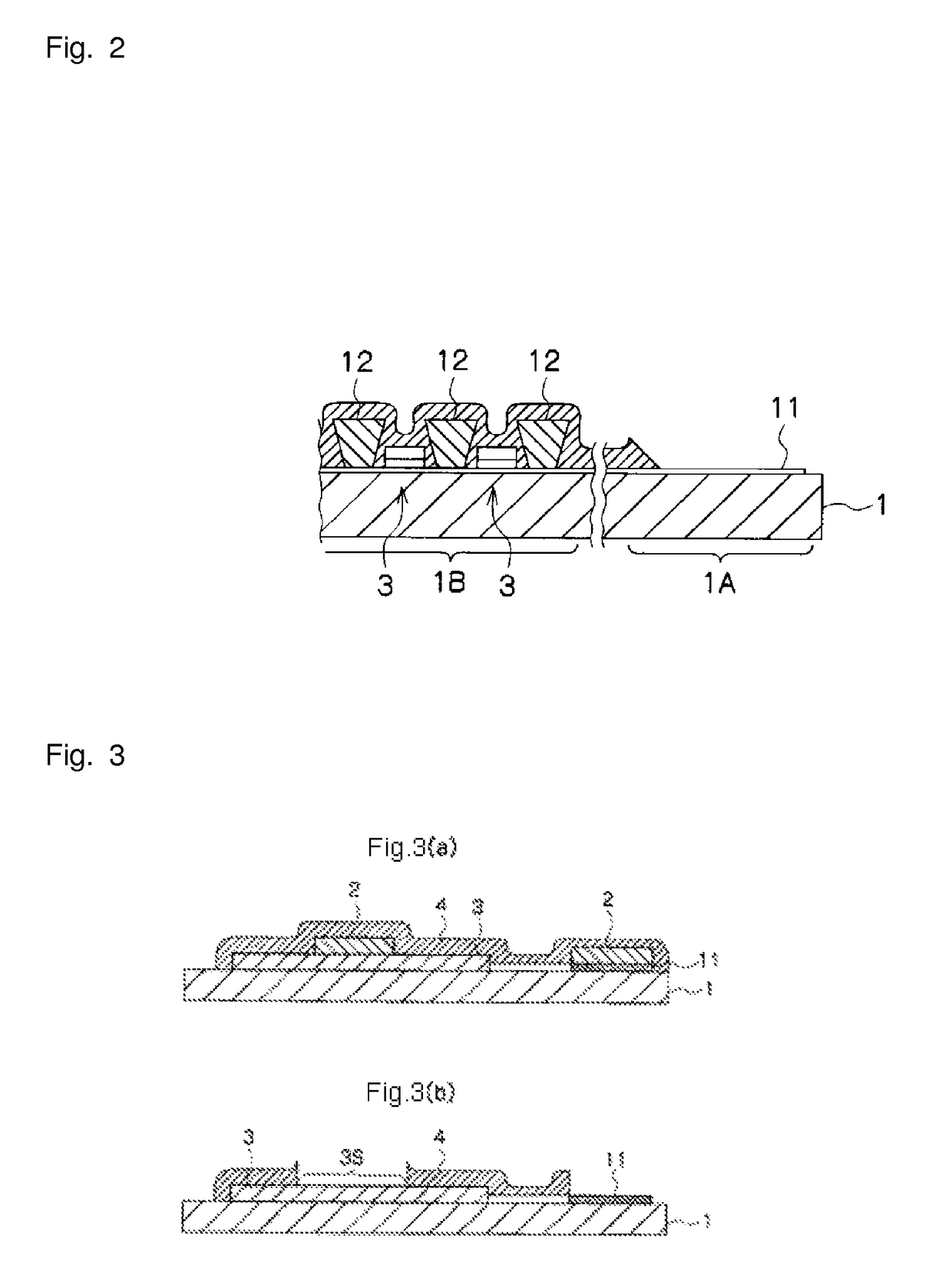
[0015]Embodiments of the present invention are explained below with reference to the drawings. The embodiments of the present invention include contents shown in the figures but are not limited to only the contents. FIG. 1 is an explanatory diagram showing a method for manufacturing an electronic device according to an embodiment of the present invention. The method for manufacturing an electronic device according to the embodiment of the present invention includes: a step of coating a substrate 1 partially with a partially coating member 2; a step of forming elements 3 on the substrate 1; a step of forming a coating film 4 on the substrate 1 to cover the elements 3 and the partially coating member 2; and a step of forming a crack in the coating film 4 on the partially coating member 2. The elements are constituent elements used in an electronic circuit and include not only an active element but also a passive element. The elements also include an organic semiconductor, a light-emit...


PUM

PropertyMeasurementUnit
work functionaaaaaaaaaa
shrinkage ratesaaaaaaaaaa
anisotropic conductiveaaaaaaaaaa

Abstract

When a coating film 4 is formed on a substrate 1, on which elements 3 are formed, by an ALD film forming method or the like, the coating film 4 is partially removed in a simple step. A method for manufacturing an electronic device includes a step of coating the substrate 1 partially with a partially coating member 2, a step of forming the elements 3 on the substrate 1, a step of forming the coating film 4 on the substrate 1 to cover the elements 3 and the partially coating member 2, and a step of forming a crack 4A in the coating film 4 on the partially coating member 2.

Description

TECHNICAL FIELD[0001]The present invention relates to a method for manufacturing an electronic device.RELATED ART[0002]There is known an electronic device including a coating film that covers an element formed on a substrate. For example, an organic EL device includes, in order to seal an organic EL element on a substrate, a coating film (a sealing film) that covers the organic EL element. The electronic device includes a connection terminal on the substrate. The electronic device including the coating film is disposed on the substrate in a state in which the connection terminal is exposed from the coating film.[0003]A method for manufacturing an organic EL device described in Patent Document 1 includes: a step of, after forming an anode and a connection terminal for external circuit connection on a substrate, provisionally compression-bonding, on the connection terminal, an anisotropic conductive adhesive tape attached with a protection laminate for connecting the connection termin...

Claims


Application Information

Patent Timeline
Patent Type & Authority Patents(United States)
IPC IPC(8): H01L51/56C23C16/455B05D1/26H01L51/52H01L27/32H01L23/31
CPCH01L51/56B05D1/26C23C16/45525H01L51/5253H01L23/3171H01L27/3246H01L27/3283H01L2924/0002H01L2924/00H10K59/122H10K59/173H10K50/844H10K71/00
Inventor SUGAHARA, JUNOHAZAMA, HIDETAKATANAKA, SHINSUKENARA, HIROMUTAN, HIROKI
Owner PIONEER CORP
Why Eureka
Try Eureka