Semiconductor device

a technology of semiconductor devices and dielectric devices, applied in the direction of logic circuits, pulse techniques, electrical pulse generator details, etc., can solve the problems of increased leakage current at low voltage, leakage current may occur, and the device may not normally operate under low-voltage operation, so as to reduce or prevent a leakage current

Active Publication Date: 2017-08-01
SK HYNIX INC
View PDF8 Cites 0 Cited by
  • Summary
  • Abstract
  • Description
  • Claims
  • Application Information

AI Technical Summary

Benefits of technology

[0005]Various embodiments of the invention are directed to a semiconductor device capable of reducing a leakage current of a main driving unit during a standby mode of the semiconductor device operating at a low voltage.
[0025]In the other embodiment, a semiconductor device may include: a main driving unit suitable for outputting input data; and a semiconductor bias controller suitable for transmitting the input data to the main driving unit during an active mode and reducing or preventing a leakage current of the main driving unit during a standby mode that the semiconductor device operates at a low voltage.

Problems solved by technology

However, when general elements which are not designed to operate at a low voltage are employed in a semiconductor device, the semiconductor device may not be normally operated under low-voltage.
Furthermore, even in elements which are designed to operate at a low voltage, a leakage current may occur.
Also, even if a low-voltage transistor having a low threshold voltage is used, a leakage current may be increased at low voltage.

Method used


Image

  • Semiconductor device
  • Semiconductor device
  • Semiconductor device

Examples


Embodiment Construction

[0028]Various embodiments of the invention will be described below in more detail with reference to the accompanying drawings. The present invention may, however, be embodied in different forms and should not be construed as limited to the embodiments set forth herein. Rather, these embodiments are provided so that this disclosure will be thorough and complete. Throughout the disclosure, like reference numerals refer to like parts throughout the various figures and embodiments of the present invention.

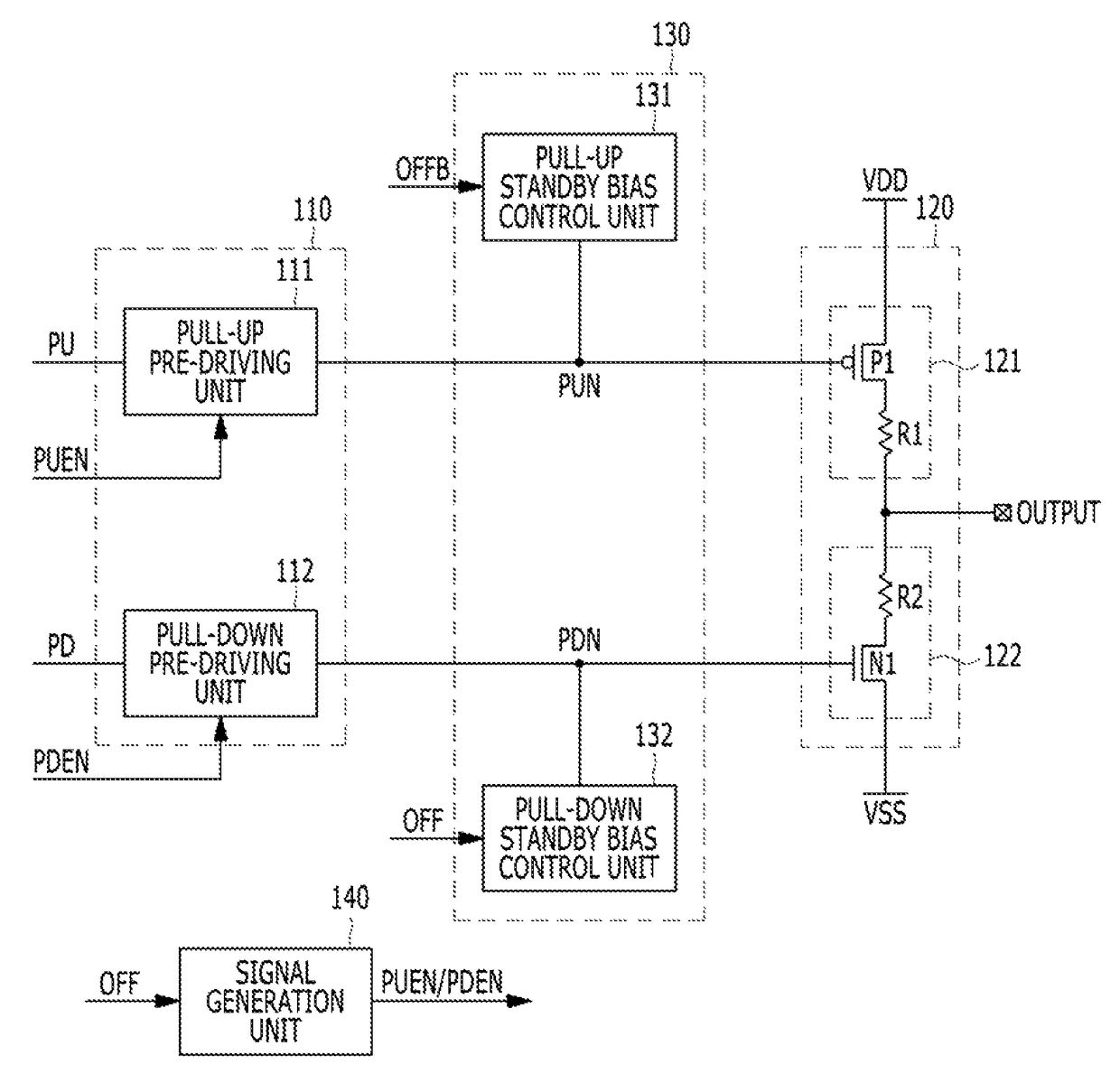
[0029]FIG. 1 is a configuration diagram of a semiconductor device according to an embodiment of the present invention.

[0030]Referring to FIG. 1, the semiconductor device may include a pre-driving unit 110, a main driving unit 120, and a bias control unit 130.

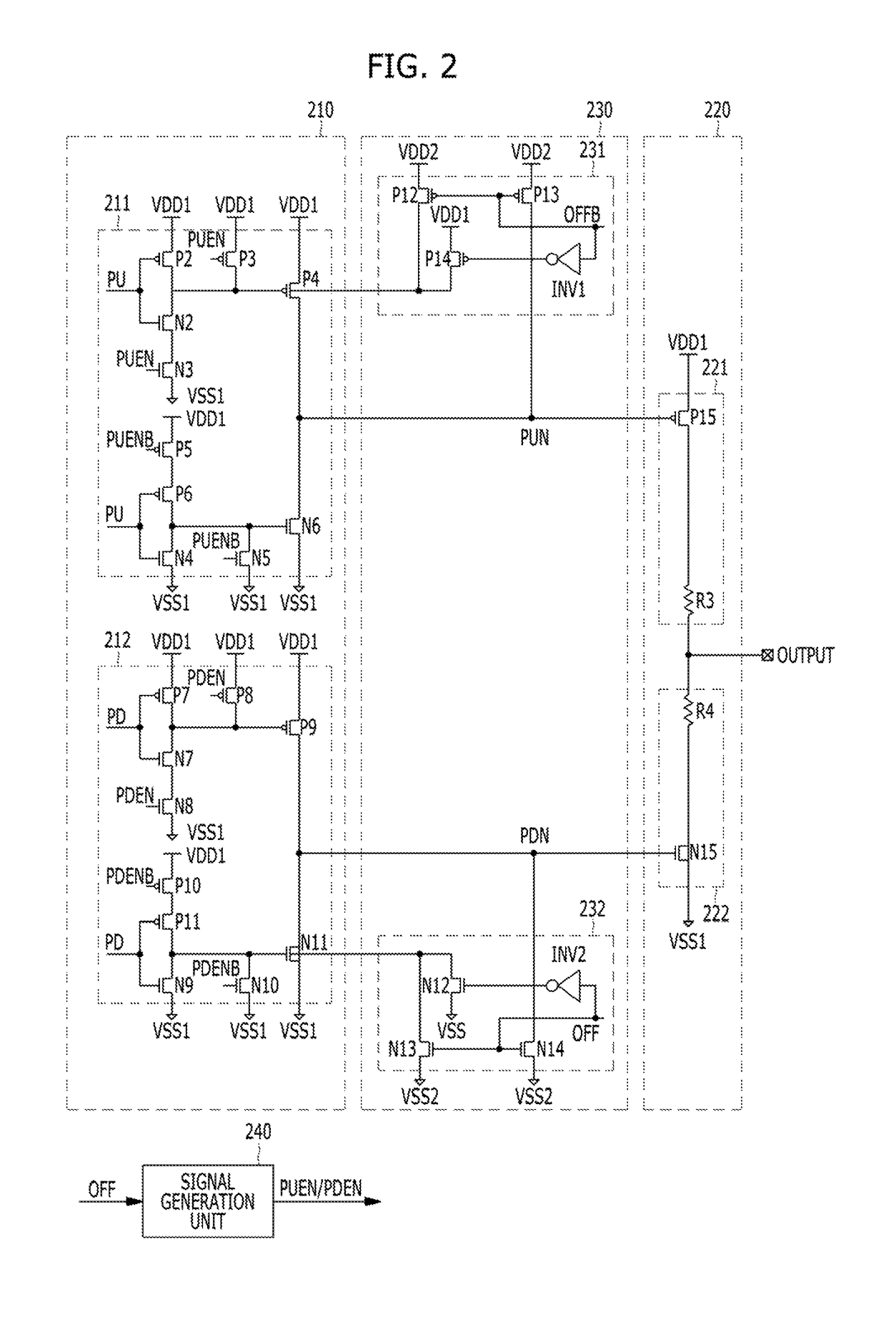
[0031]The pre-driving unit 110 may include a pull-up pre-driving unit 111 and a pull-down pre-driving unit 112. The pull-up pre-driving unit 111 may output input data PU to a first node PUN in response to a control signal PUEN. The...


PUM


Abstract

A semiconductor device may include: a pre-driving unit suitable for transmitting input data to a first node in response to a first control signal; a main driving unit suitable for outputting the input data transmitted to the first node, using a first voltage as a driving voltage; and a bias control unit suitable for supplying a second voltage to the first node in response to a second control signal, the second voltage having a different level from the first voltage.

Description

BACKGROUND[0001]1. Field[0002]The present invention relates generally to a semiconductor technology, and more particularly to a semiconductor device which performs a data output operation.[0003]2. Description of the Related Art[0004]Semiconductor devices have been gradually improving in terms of speed, integration, and power consumption. Generally, in order to achieve higher speed and lower power consumption, various elements employed in a semiconductor device must be typically operated at a low voltage. However, when general elements which are not designed to operate at a low voltage are employed in a semiconductor device, the semiconductor device may not be normally operated under low-voltage. Furthermore, even in elements which are designed to operate at a low voltage, a leakage current may occur. For example, a general transistor having a high threshold voltage may not operate in response to a low voltage. Also, even if a low-voltage transistor having a low threshold voltage is ...

Claims


Application Information

Patent Timeline
Patent Type & Authority Patents(United States)
IPC IPC(8): H03K17/00H03K3/01H03K3/356
CPCH03K3/01H03K3/356113H03K19/018521
Inventor KIM, JAE-HEON
Owner SK HYNIX INC
Why Eureka
Try Eureka