

Elastic wave device and manufacturing method for same
a technology of elastic wave and manufacturing method, which is applied in the direction of impedence network, electrical apparatus, etc., can solve the problems of reducing the ability to handle electric power, reducing the processing accuracy of idt electrodes, and deteriorating wiring resistance, so as to facilitate the electrode design of elastic wave devices and realize elastic wave devices. , the effect of small siz
Active Publication Date: 2017-08-29
MURATA MFG CO LTD
View PDF12 Cites 72 Cited by
- Summary
- Abstract
- Description
- Claims
- Application Information
AI Technical Summary
Benefits of technology
The patent describes an elastic wave device with improved resonance and filter characteristics. The device uses a film thickness of the IDT electrode that satisfies a certain condition to reduce electrical resistance and improve the coupling coefficient of the secondary mode. Additionally, the device has a small power flow angle, which facilitates electrode design and reduces interference from spurious modes. Overall, the device has better performance and reliability.
Problems solved by technology
This causes the problem that a very high level of processing accuracy is required to form the IDT electrode.
Another problem is that, because the electrode finger width is very narrow, wiring resistance may deteriorate, or an electric power handling capability may decrease.
Method used
View moreImage
Smart ImageViewing Examples

Examples
example 1
[0162]An elastic wave device was constructed in a similar structure to that in the first preferred embodiment.
example 2
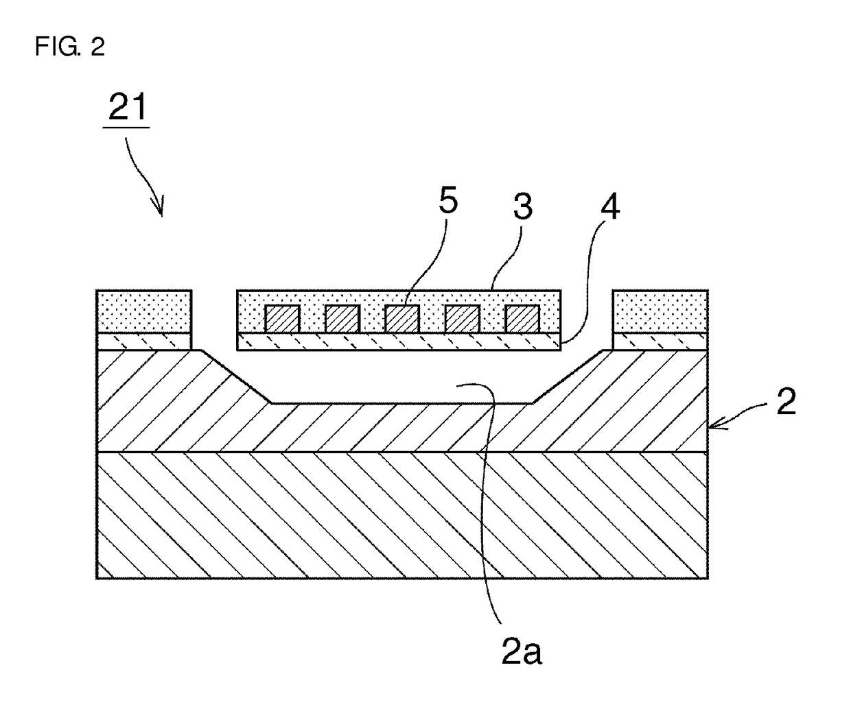
[0163]An elastic wave device was fabricated as in the third preferred embodiment, illustrated in FIG. 3A, except that it includes a SiO2 film having a thickness of about 0.05λ as the dielectric film 3.
example 3
[0164]An elastic wave device was fabricated as in the third preferred embodiment, illustrated in FIG. 3A, except that it includes a SiN film having a thickness of about 0.05λ as the dielectric film 3.
Login to View More PUM
| Property | Measurement | Unit |
|---|---|---|
| propagation velocity | aaaaa | aaaaa |
| terminal impedance | aaaaa | aaaaa |
| thickness | aaaaa | aaaaa |
Abstract
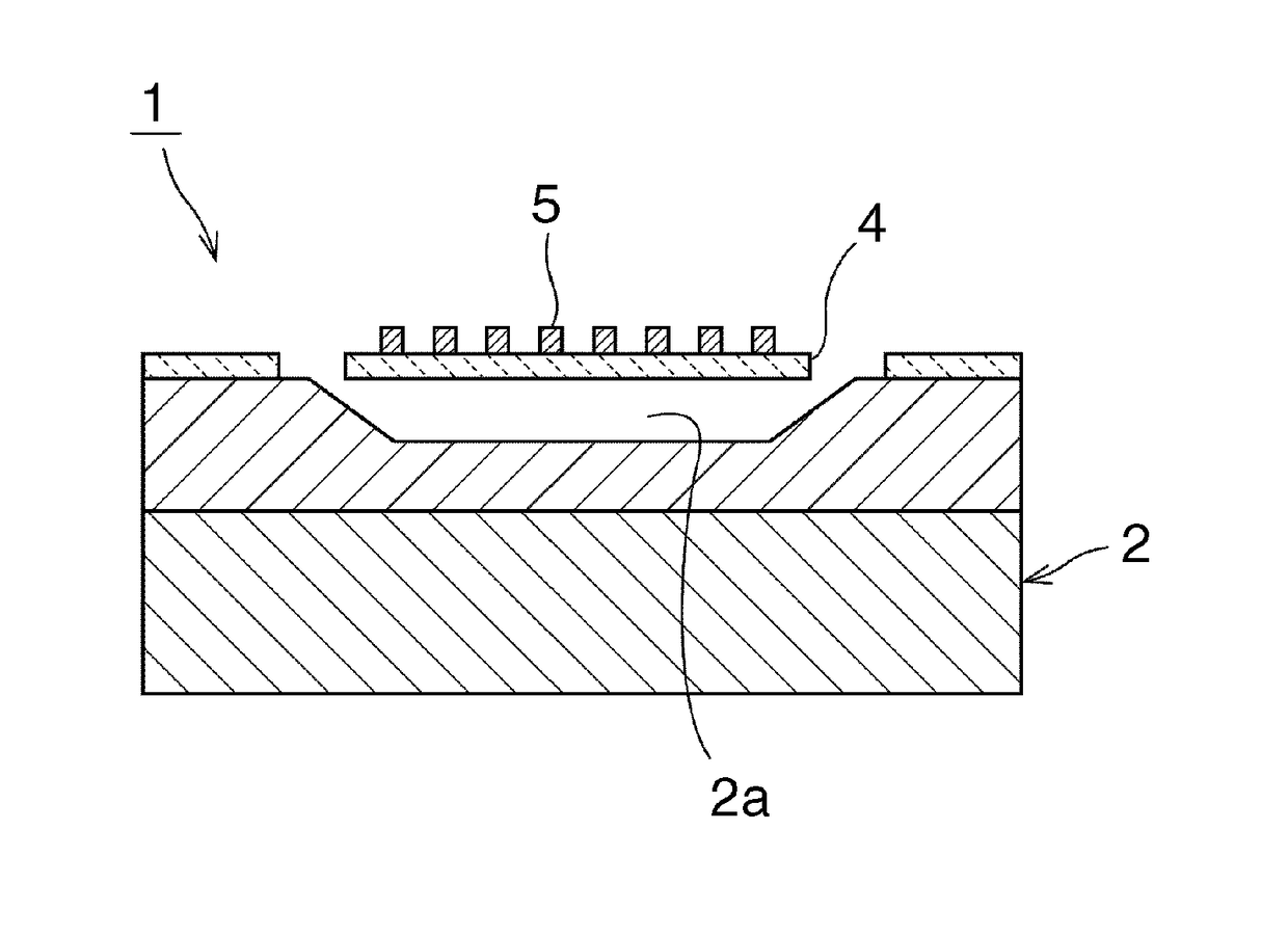
An elastic wave device includes a support layer with a through-hole or a recess opened at an upper surface thereof, a piezoelectric thin film arranged on the support layer to extend above the recess or the through-hole of the support layer, and an IDT electrode defined on at least one of upper and lower surfaces of the piezoelectric thin film in a region of the piezoelectric thin film, the region extending above the recess, or the through-hole. A secondary mode of a plate wave, which contains a U1 component as a main component, is utilized. The piezoelectric thin film is made of LiTaO3, and Euler angles (φ, θ, ψ) of the LiTaO3 fall within specific ranges.
Description
BACKGROUND OF THE INVENTION[0001]1. Field of the Invention[0002]The present invention relates to an elastic wave device including a piezoelectric thin film, and to a manufacturing method for the elastic wave device. More particularly, the present invention relates to an elastic wave device using a higher-order mode of a plate wave called a Lamb wave, and to a manufacturing method for the elastic wave device.[0003]2. Description of the Related Art[0004]Recently, an elastic wave device using a piezoelectric thin film has been proposed with the development of, e.g., communication apparatuses operating at higher frequencies. For realizing operation at a higher frequency, it is required to increase the acoustic velocity of an elastic wave in a piezoelectric substrate. From that point of view, attention is focused on an elastic wave device using a plate wave with a high acoustic velocity.[0005]The term “plate wave” means an elastic wave propagating through a medium sandwiched between two ...
Claims
Login to View More Application Information
Patent Timeline
 Patent Type & AuthorityPatents(United States)
IPC IPC(8): H03H9/02H03H9/25H03H3/02H03H3/08
CPCH03H9/25H03H3/02H03H9/02228H03H9/02559H03H9/02574H03H9/02834H03H3/08Y10T29/42
InventorKANDO, HAJIMEKIDO, SYUNSUKEOKADA, KEIJIWATANABE, MUNEHISA
OwnerMURATA MFG CO LTD