
Semiconductor device having a first circuit board mounted with a plurality of semiconductor elements and a second circuit board mounted with a plurality of electronic components

a semiconductor device and circuit board technology, applied in the direction of coupling device connection, electrical apparatus casing/cabinet/drawer, association of printed circuit non-printed electric components, etc., can solve the problem of thermal disadvantage of the semiconductor device, and achieve the effect of reducing the degree of rotation (degree of rotation) of the external terminal connecting portion and easy carrying of curren

Active Publication Date: 2017-09-05
TOYOTA IND CORP
View PDF15 Cites 2 Cited by
  • Summary
  • Abstract
  • Description
  • Claims
  • Application Information

AI Technical Summary

Benefits of technology

The present invention provides a semiconductor device with a small-sized connecting terminal that allows peripheral electronic components to be compactly mounted on the circuit board without a need for a large mount region on the circuit board. The connecting terminal includes an external terminal connecting portion and a substrate-fixed portion that are eccentrically located when viewed from the direction in which the first circuit board and the second circuit board are opposed. The reduced sectional area portion of the connecting terminal allows the top end surface to overlap a portion of the electronic component adjoining the reduced sectional area portion, allowing the electronic component to be arranged close enough to the external terminal connecting portion. The external terminal connecting portion has a plurality of straight regions that prevent rotation when connected to the substrate-fixed portion, ensuring accuracy in positioning the external terminal connecting portion.

Problems solved by technology

When the top end surface area is small, therefore, the cylinder portion (end portion) is likely to generate heat which is thermally disadvantageous to the semiconductor device.

Method used


Image

  • Semiconductor device having a first circuit board mounted with a plurality of semiconductor elements and a second circuit board mounted with a plurality of electronic components
  • Semiconductor device having a first circuit board mounted with a plurality of semiconductor elements and a second circuit board mounted with a plurality of electronic components
  • Semiconductor device having a first circuit board mounted with a plurality of semiconductor elements and a second circuit board mounted with a plurality of electronic components

Examples


Embodiment Construction

[0026]The embodiment of the present invention will be described in detail referring to the attached drawings. In the description, the same component or the component having the same function is denoted with the same reference sign and repeated description thereof will be omitted. Dimensional ratios in each drawing may be different from the actual dimensional ratios.

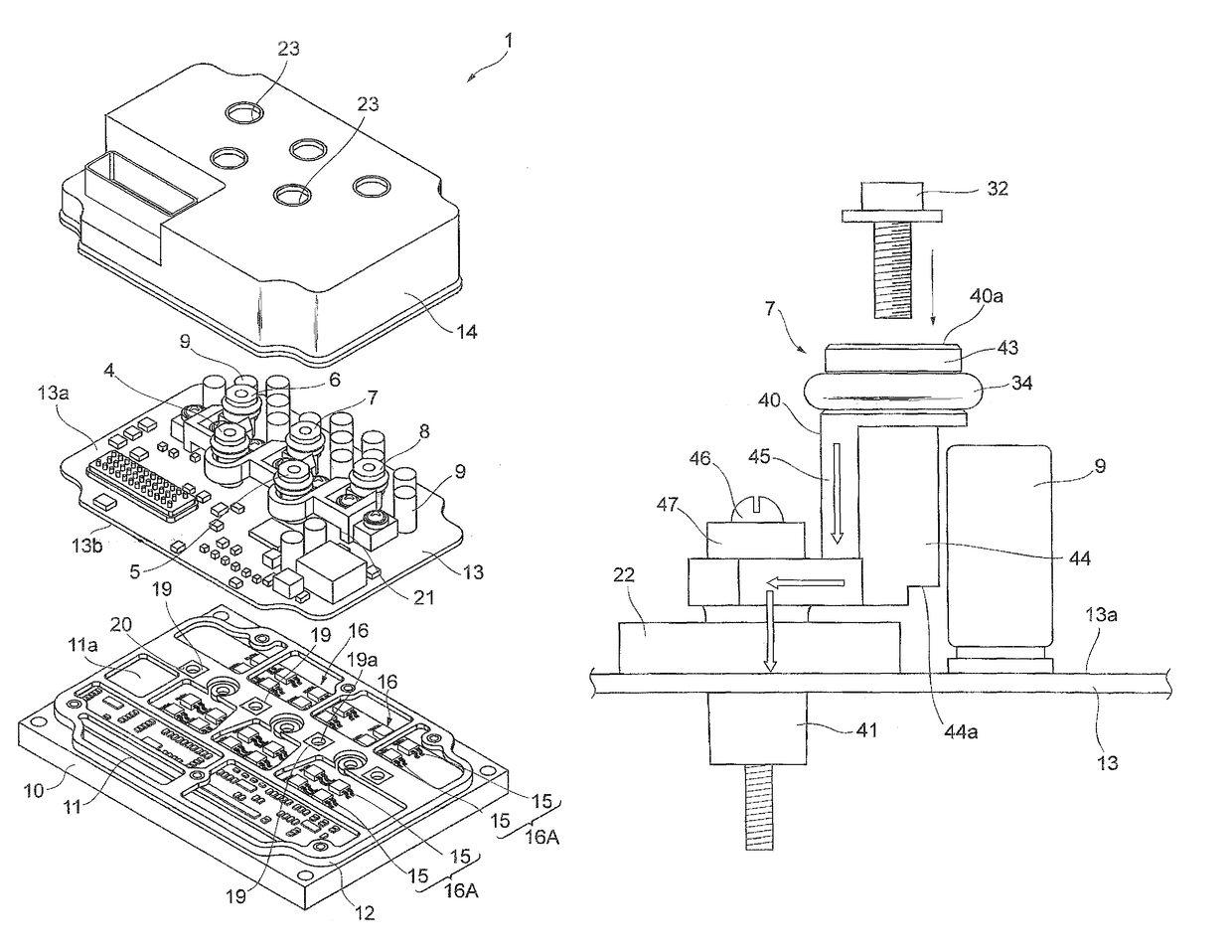
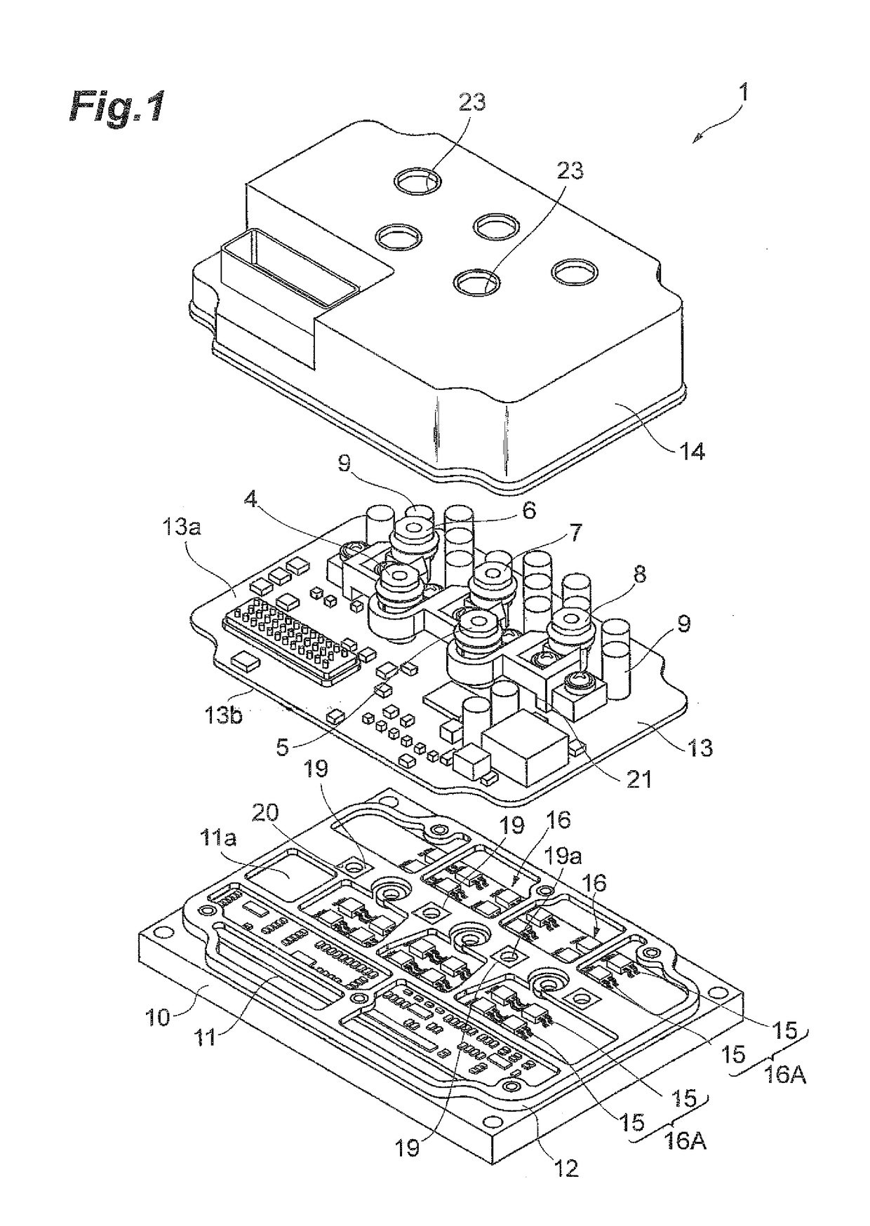
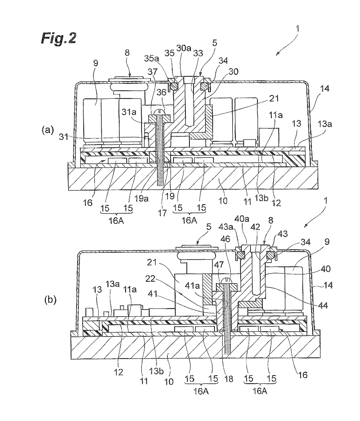
[0027]FIG. 1 is an exploded perspective view illustrating an inverter device according to the embodiment. FIG. 2 is sectional views of the inverter device illustrated in FIG. 1. In FIG. 2, (a) is a sectional view taken along the line IIA-IIA in FIG. 4 and (b) is a sectional view taken along the line IIB-IIB in FIG. 4. The inverter device 1 of the embodiment is, for example, a three-phase inverter device for driving a three-phase AC motor.

[0028]FIG. 3 is a circuit diagram of the inverter device 1. As illustrated in FIG. 3, the inverter device 1 includes a main circuit 2, a control circuit 3 for controlling the main circuit...


PUM


Abstract

A connecting terminal includes an external terminal connecting portion, having an end surface to connect an external terminal thereto and located at a second principal surface side of a second circuit board faces, and a substrate-fixed portion which is securely connected to a first circuit board. A seal attachment portion is provided on a portion of the external terminal connecting portion including the end surface to attach thereto a seal member to seal a gap between the portion and the case. The connecting terminal includes a reduced sectional area portion having a sectional area smaller than an area of the top end surface in a region close to a plurality of electronic components arranged on the second circuit board on the external terminal connecting portion. The reduced sectional area portion is provided from the seal attachment portion to an end in the opposite side of the end surface.

Description

CROSS-REFERENCE TO RELATED APPLICATIONS[0001]This application claims priority to Japanese Application No. P2014-006582 filed Jan. 17, 2014, the disclosure of which is incorporated herein by reference in its entirety.BACKGROUND OF THE INVENTION[0002]Field of the Invention[0003]The present invention relates to a semiconductor device.[0004]Related Background Art[0005]There are known semiconductor devices such as a semiconductor device discussed in JP Registered Utility Model Publication No. 3173512. The semiconductor device discussed in JP Registered Utility Model Publication No. 3173512 includes a main circuit board mounted with a plurality of semiconductor elements composing a main circuit, a capacitor substrate which is closely arranged on the main circuit board and mounted with a plurality of capacitors, and a control circuit board which is arranged on the capacitor substrate with a distance provided in between and mounted with a control circuit controlling the main circuit. A posi...

Claims


Application Information

Patent Timeline
Patent Type & Authority Patents(United States)
IPC IPC(8): H05K5/00H01R12/51H05K1/18H05K7/14H05K1/14H02M7/00H01R13/631H01R13/52H05K3/32
CPCH05K1/181H01R12/515H05K7/1432H01R13/5202H01R13/6315H02M7/003H05K1/144H05K3/325H05K2201/09063H05K7/14322H05K7/14329
Inventor KONTANI, KAZUYOSHIDOJIRI, ATSUSHI
Owner TOYOTA IND CORP
Learn More