Electronic circuits

a technology of electronic circuits and circuits, applied in logic circuits, electric pulse generators, pulse counters, etc., can solve problems such as difficult combining the two into a single manufacturable process, mismatch in achievable performance, and critical lack of robust cmos capability

Active Publication Date: 2017-09-19
PRAGMATIC PRINTING
View PDF11 Cites 0 Cited by
  • Summary
  • Abstract
  • Description
  • Claims
  • Application Information

AI Technical Summary

Benefits of technology

[0010]It is an aim of certain embodiments of the invention to solve, mitigate or obviate, at least partly, at least one of the problems and / or disadvantages associated with the prior art. Certain embodiments aim to provide at least one of the advantages described below.
[0033]It will be appreciated that certain embodiments of the invention can be described as incorporating ‘NCMOS’ technology, which is a novel quasi-CMOS design / technology made entirely from NMOS devices, invented by the present inventors. Compared to flexible CMOS, this provides major benefits in terms of manufacture because NMOS processing can be directly applied.

Problems solved by technology

However, in flexible electronics NMOS is currently state-of-the-art and the lack of robust CMOS capability is a critical issue.
In flexible electronics significant effort has been put into both NMOS and PMOS but there is a mismatch in achievable performance (e.g. mobilities).
Complementary materials require very different deposition and patterning processes (e.g. solution-deposition vs. vacuum-deposition), thus combining the two into a single manufacturable process is very challenging.
The three NMOS variants, as illustrated in FIG. 1a, all have benefits and drawbacks (footprint, power efficiency, noise margin), and are used today in “Flexible Electronics” due to the absence of a commercially viable manufacturing route to CMOS.
However, this limits the ease of design as well as the degree of integration and complexity that can be achieved.

Method used


Image

  • Electronic circuits
  • Electronic circuits
  • Electronic circuits

Examples


Embodiment Construction

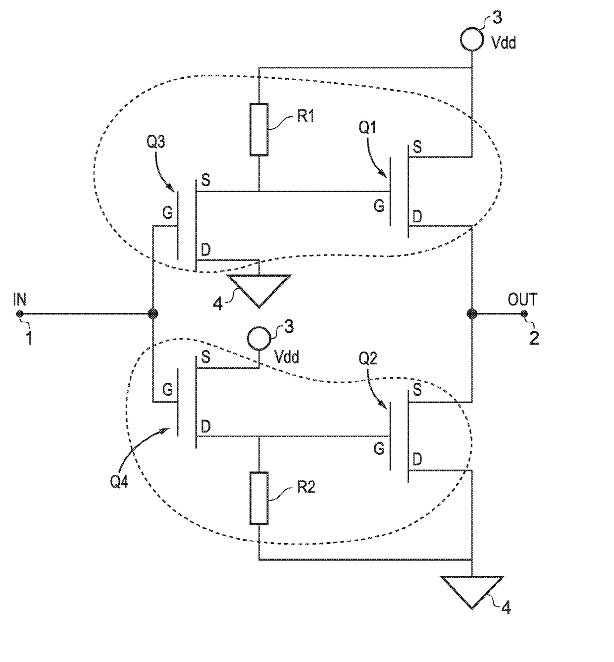
[0061]FIG. 4 illustrates an inverter embodying the present invention, and incorporating the NCMOS concept / technology invented by the present inventors.

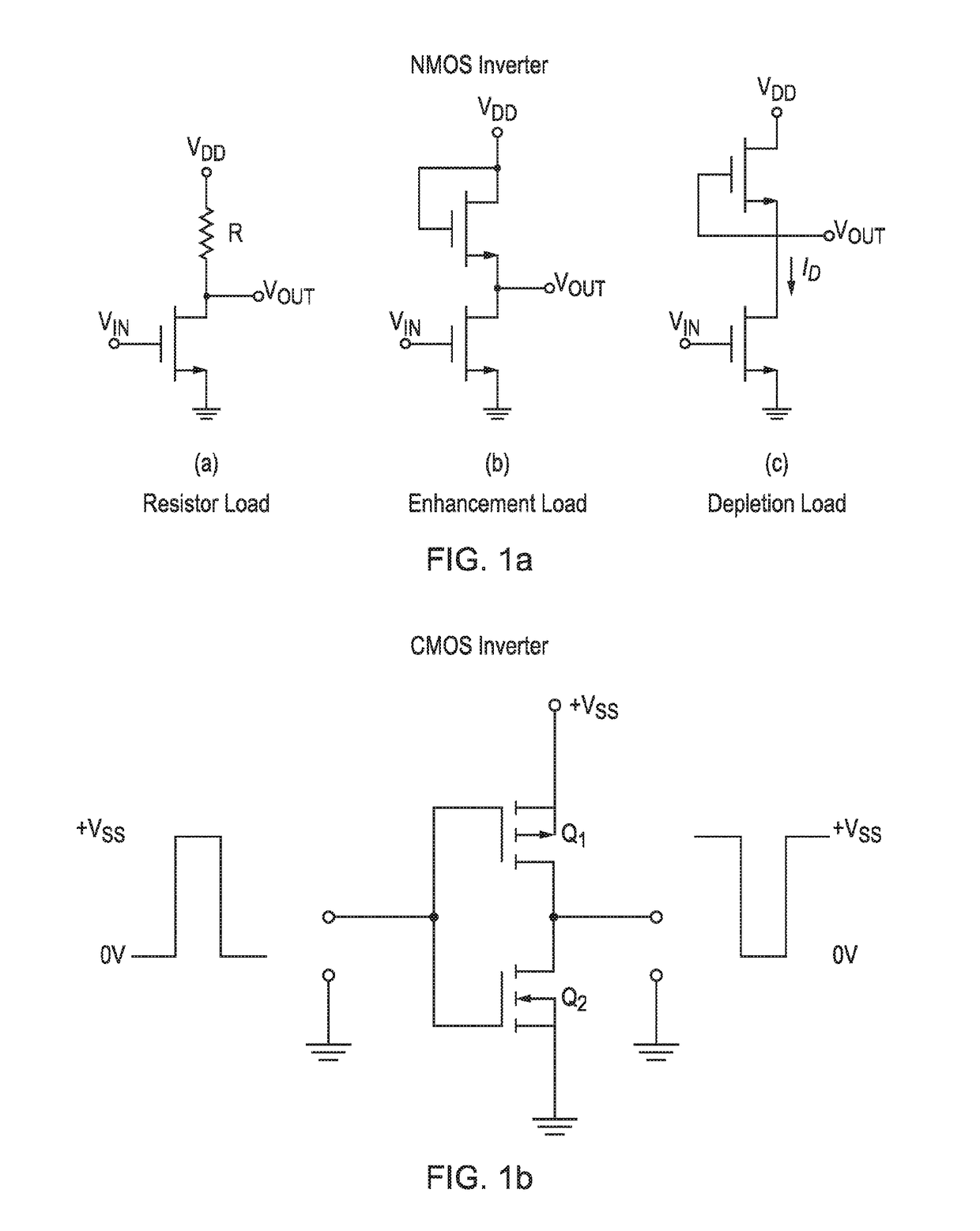
[0062]The device comprises four NMOS transistors (Q1, Q2, Q3, and Q4) and two loads R1 and R2, which can also be described as polarising load elements (and can take the form, in certain embodiments, of resistors, N-type enhancement loads or N-type depletion loads). Essentially it is a hybrid between NMOS and CMOS, hence the name NCMOS.

[0063]In the terminology of claim 1, Q1 is the first FET, Q2 is the second FET, and so on. The first supply rail 3 is Vdd in this example, and the second supply rail 4 is Vss or ground. Input terminal 1 and output terminal 2 are labelled, and the source, drain, and gate terminals of each of the FETs are labelled, as S, D, and G respectively. The connections between the various terminals are as defined in claim 1. In this example, the respective connections between the source and drain terminals of the fi...


PUM


Abstract

An electronic circuit comprises: an input terminal; an output terminal; first and second supply rails; first, second, third, and fourth field effect transistors, FETs, each of a first type and each having respective gate, source and drain terminals; and first and second loads. The source of the first FET is connected to the first supply rail, the drain of the first FET and the source of the second FET are connected to the output terminal, the drain of the second FET is connected to the second supply rail, the gate of the third FET and the gate of the fourth FET are connected to the input terminal, the drain of the third FET is connected to the second supply rail, the first load is connected between the first supply rail and the source of the third FET, and the second load is connected between the drain of the fourth FET and the second supply rail. In one aspect of the invention, the gate of the first FET is connected to a node between the source of the third FET and the first load such that a voltage at the source of the third FET is applied to the gate of the first FET, and the gate of the second FET is connected to a node between the drain of the fourth FET and the second load such that a voltage at the drain of the fourth FET is applied to the gate of the second FET.

Description

CROSS REFERENCE TO RELATED APPLICATIONS[0001]This is the U.S. National Stage of International Application No. PCT / GB2014 / 052175, filed Jul. 16, 2014, which in turn claims the benefit and priority to United Kingdom Application No. GB1312809.5, filed Jul. 17, 2013.[0002]The present invention relates to electronic circuits, and in particular, although not exclusively, to electronic logic circuits, for example for use as building blocks in signal processing circuits and apparatus. Certain embodiments relate to flexible logic circuits.BACKGROUND[0003]Conventional semiconductor devices and related EDA tools / libraries are mostly based around CMOS logic circuits.[0004]CMOS uses complementary n-type and p-type transistors, and displaced the previous NMOS (n-type) technologies in the 1980s due to better power efficiency, higher noise margin, improved fan-out and easier integration. However, in flexible electronics NMOS is currently state-of-the-art and the lack of robust CMOS capability is a ...

Claims


Application Information

Patent Timeline
Patent Type & Authority Patents(United States)
IPC IPC(8): H03K3/03H03K23/00H03K19/20H03K3/356H03K19/0944H03K17/16H03K3/037
CPCH03K19/0944H03K3/037H03K3/0315H03K3/356017H03K17/16H03K19/09441H03K19/20H03K23/002
Inventor DE OLIVEIRA, JOAOWHITE, SCOTT DARRENRAMSDALE, CATHERINE
Owner PRAGMATIC PRINTING
Why Eureka
Try Eureka