
Static semiconductor memory device using a single global data line

Active Publication Date: 2017-10-10
SOCIONEXT INC
View PDF14 Cites 2 Cited by
  • Summary
  • Abstract
  • Description
  • Claims
  • Application Information

AI Technical Summary

Benefits of technology

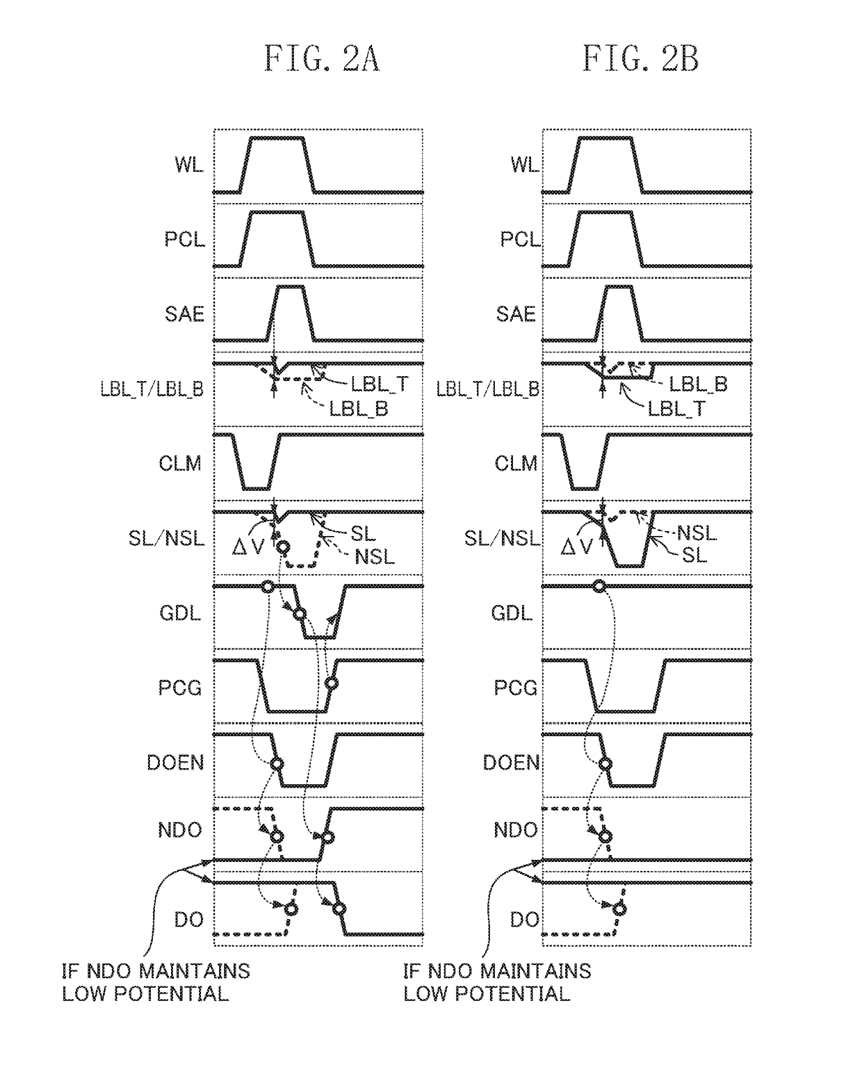
The present disclosure provides a semiconductor memory device that can maintain the global data line at the normal High potential level, even when there is leakage current. This prevents data from being read erroneously onto the global data line and allows for proper resetting of output data. Additionally, balancing the load capacities of the connection nodes between the differential amplifier and local bit lines reduces the chances of the differential amplifier operating erroneously. Overall, this semiconductor memory device is less likely to operate erroneously and provides a more reliable data transfer.

Problems solved by technology

As the storage capacity of those memories is increased, however, the number of memory cells to be connected to a single bit line also needs to be increased, which imposes a heavier and heavier load capacity on each bit line, thus inhibiting the memory cells from further increasing their operating speeds as required.
As a result, the output level of the inverter that should be Low is raised to a High potential level to turn the transistor ON unintentionally.
Thus, data may be read erroneously on the global bit line.
Particularly if the inverter has varying threshold values such that the level of its input is easily determined to be Low or if there is little potential difference between the pair of bit lines, there are higher chances of the storage device operating erroneously.
In this case, if the potential of the global bit line has decreased to a lower level, the drivability of the output circuit may deteriorate too much to have the output data reset normally by the output circuit.
As a result, the storage device may operate erroneously.
Moreover, since an inverter is connected to one of each pair of local bit lines, the load capacities of respective connection nodes between the pair of local bit lines and the differential amplifier are so imbalanced that the differential amplifier tends to operate erroneously, which is another concern about the conventional storage device.

Method used


Image

  • Static semiconductor memory device using a single global data line
  • Static semiconductor memory device using a single global data line
  • Static semiconductor memory device using a single global data line

Examples


first embodiment

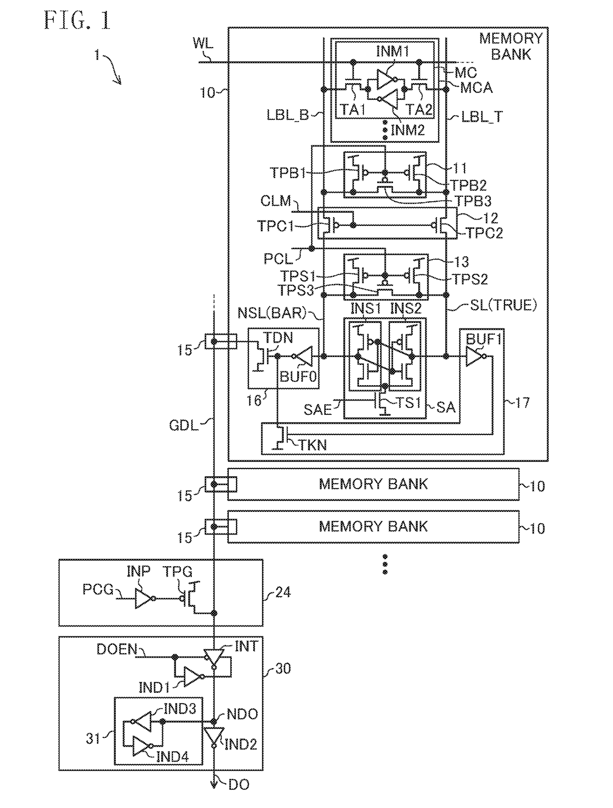
[0036]FIG. 1 illustrates a configuration for a semiconductor memory device according to a first embodiment. A semiconductor memory device 1 according to this embodiment has a hierarchical bit line structure, and is configured to read data using a global data line GDL having a single-ended configuration. Specifically, the semiconductor memory device 1 includes a plurality of memory banks 10, a single global data line GDL, a global precharge circuit 24, and an I / O circuit 30.

[0037]Each of the memory banks 10 includes: a memory cell array MCA including a plurality of memory cells MC arranged in columns and rows; a word line WL; a pair of local bit lines LBL_B, LBL_T; a bit line precharge circuit 11; a column selector 12; a pair of sense lines NSL, SL; a sense line precharge circuit 13; a differential amplifier SA; a connector 15; and first and second output circuits 16, 17.

[0038]Each of the memory cells MC may be configured as a static random access memory (SRAM), for example, and incl...

second embodiment

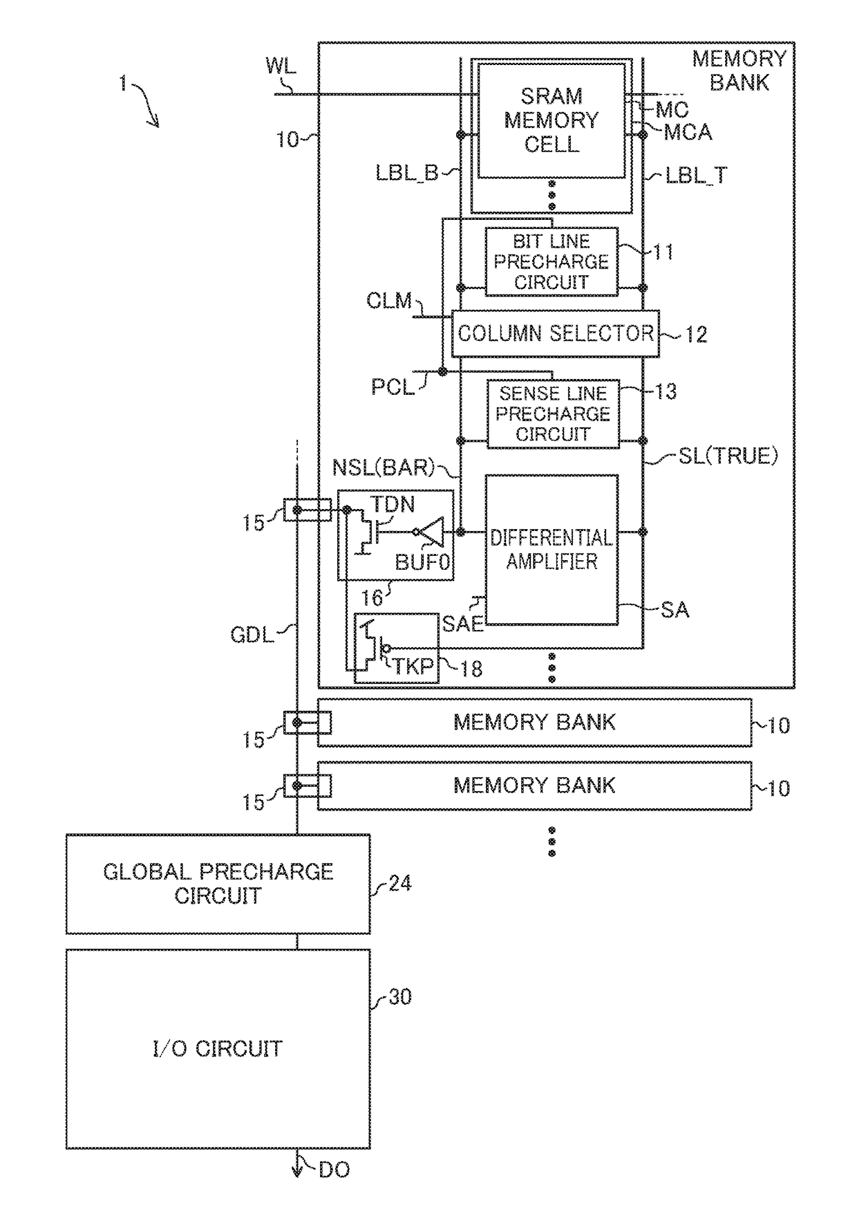
[0084]FIG. 3 illustrates a configuration for a semiconductor memory device according to a second embodiment. In FIG. 3, the SRAM memory cells MC, the bit line precharge circuit 11, the column selector 12, the sense line precharge circuit 13, the differential amplifier SA, the global precharge circuit 24, and the I / O circuit 30 are illustrated as simple blocks, because they have the same configuration as their counterparts shown in FIG. 1.

[0085]The following description of this embodiment will be focused on the differences from the first embodiment. A second output circuit 18 included in each memory bank 10 according to this embodiment selectively outputs, according to the potential level of the sense line SL, a second potential (such as the voltage VDD) having High level as a second type of logic to the connector 15. Specifically, the output circuit 18 includes a Pch transistor TKP, one terminal of which is connected to the voltage VDD, another terminal of which is connected to the ...

third embodiment

[0096]FIG. 4 illustrates a configuration for a semiconductor memory device according to a third embodiment. The semiconductor memory device 1 of this embodiment further includes a predischarge circuit 25 which precharges the global data line GDL to a Low potential level (i.e., predischarges it), which is a major difference from the second embodiment. Thus, the following description of the third embodiment will be focused on the differences from the second embodiment.

[0097]In the memory bank 10 shown in FIG. 4, a first output circuit 19 selectively outputs a High potential to the connector 15 according to the potential level of the sense line SL. Specifically, the output circuit 19 includes a Pch transistor TKP, one terminal of which is connected to the voltage VDD, another terminal of which is connected to the connector 15, and the gate of which receives the potential of the sense line SL.

[0098]A second output circuit 20 selectively outputs a Low potential to the connector 15 accord...


PUM


Abstract

A memory bank of a semiconductor memory device includes: a plurality of memory cells; first and second local bit lines; a differential amplifier configured to amplify a potential difference between the first and second local bit lines; a connector to which a global data line is connected; a first output circuit configured to selectively output, according to a potential level of the first local bit line, a first potential to the connector; and a second output circuit configured to selectively prevent, according to a potential level of the second local bit line, a potential of the connector from being affected by an output of the first output circuit and being equal to the first potential.

Description

CROSS-REFERENCE TO RELATED APPLICATION[0001]This is a continuation of International Application No. PCT / JP2014 / 005056 filed on Oct. 3, 2014, which claims priority to Japanese Patent Application No. 2013-244576 filed on Nov. 27, 2013. The entire disclosures of these applications are hereby incorporated by reference.BACKGROUND[0002]The present disclosure relates to a semiconductor memory device, and more particularly relates to a semiconductor memory device in which bit lines have a hierarchical structure.[0003]Nowadays, memories built in systems on chip (SOCs) have their storage capacity further increased to have even higher operating speeds. As the storage capacity of those memories is increased, however, the number of memory cells to be connected to a single bit line also needs to be increased, which imposes a heavier and heavier load capacity on each bit line, thus inhibiting the memory cells from further increasing their operating speeds as required. Thus, a hierarchical bit line...

Claims


Application Information

Patent Timeline
IPC IPC(8): G11C11/419G11C7/12
CPCG11C7/12G11C11/419
Inventor KOIKE, TSUYOSHI
Owner SOCIONEXT INC
Learn More