Semiconductor device

a technology of semiconductors and diodes, applied in the direction of semiconductor devices, basic electric elements, electrical equipment, etc., can solve the problems of insufficient impurity concentration on the surface, the recovery properties of diodes are contrarily reduced, and the cost reduction of inverter devices is hugely needed. to achieve the effect of improving the recovery properties of diodes

Active Publication Date: 2017-10-24
MITSUBISHI ELECTRIC CORP
View PDF12 Cites 3 Cited by
  • Summary
  • Abstract
  • Description
  • Claims
  • Application Information

AI Technical Summary

Benefits of technology

[0006]It is an object of the present invention to provide a semiconductor device in which recovery properties of a diode are improved, the semiconductor device including an IGBT and the diode formed on one semiconductor substrate.
[0008]In the semiconductor device of the present invention, the resistance element is located between the well region and the first electrode. The resistance element suppresses an injection of holes from the well region when the freewheeling diode is in an ON state. This suppresses a reverse recovery current when the freewheeling diode is turned off. Thus, the recovery properties can be improved in the semiconductor device including the freewheeling diode and the insulated gate bipolar transistor formed on the same substrate.

Problems solved by technology

However, size, weight, and cost reductions of inverter devices are greatly needed, so that a plurality of semiconductor elements are not preferably installed.
However, recovery properties of the diode are contrarily decreased, so that the impurity concentration of the surface cannot be set sufficiently high.

Method used


Image

  • Semiconductor device
  • Semiconductor device
  • Semiconductor device

Examples


Embodiment Construction

[0020]

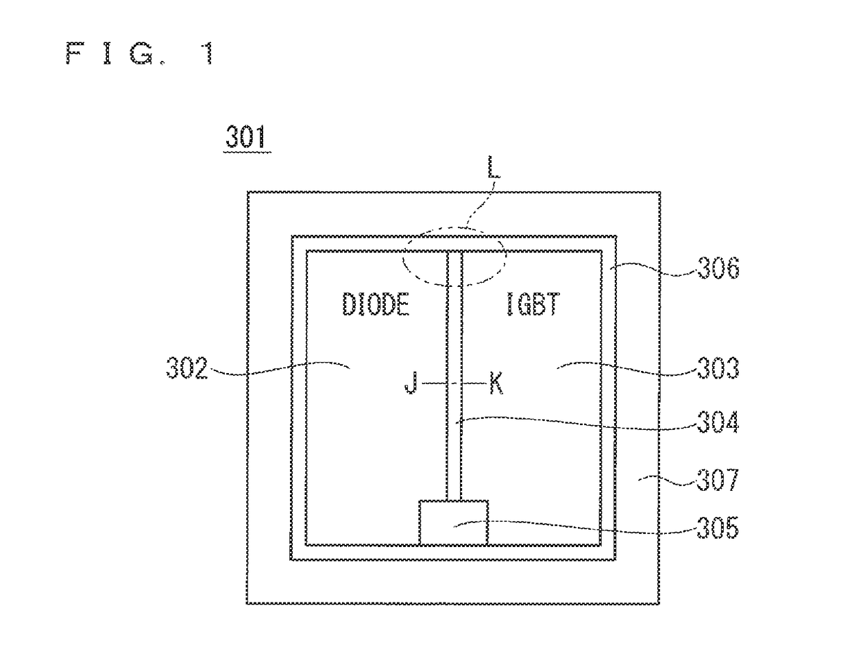
[0021]A prerequisite technology of the present invention is described before a preferred embodiment of the present invention is described. FIG. 7 is a plan view of a semiconductor device (namely, RC-IGBT 101) in the prerequisite technology. FIG. 8 is a cross-sectional view taken along an A-B line segment across a region of a diode 102 and a region of an IGBT 103 in FIG. 7. FIG. 9 is an enlarged plan view of a region C in FIG. 7.

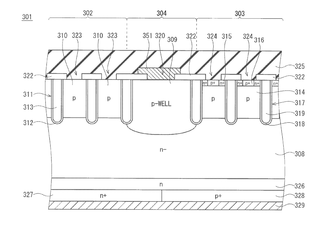
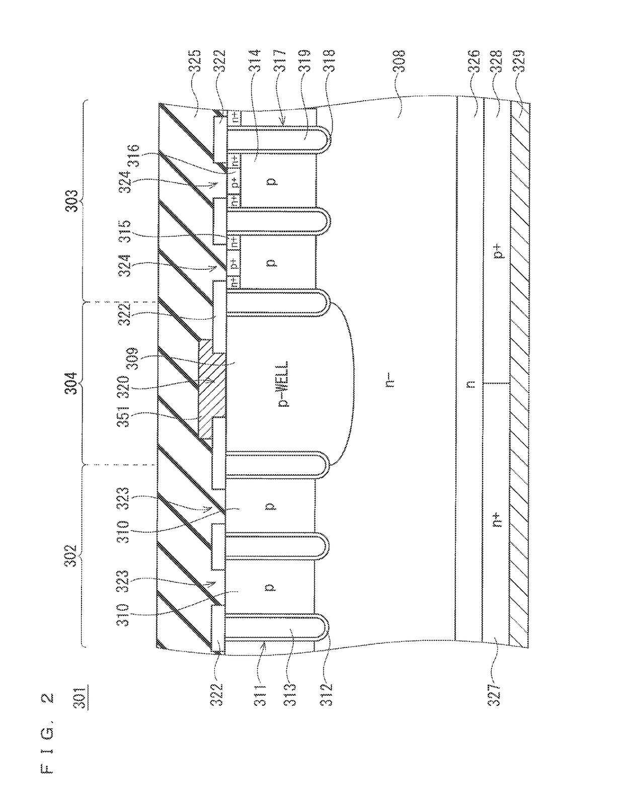
[0022]As shown in FIG. 7, the RC-IGBT 101 includes the diode 102 and the IGBT 103. A well region 104 is located between the diode 102 and the IGBT 103. A p-well 109 is located in the well region 104 so as to separate the diode 102 and the IGBT 103. The

[0023]RC-IGBT 101 further includes a gate pad region 105, a termination region 106, and a breakdown voltage holding region 107.

[0024]As shown in FIG. 8, an n− drift layer 108 common to the diode 102 and the IGBT 103 is located on a semiconductor substrate. The p-well 109 is located on an upper surface side...


PUM


Abstract

A semiconductor device of the present invention includes: an IGBT including an emitter layer on a first main surface side of a semiconductor substrate and a collector layer on a second main surface side of the semiconductor substrate; a freewheeling diode including an anode layer on the first main surface side of the semiconductor substrate and a cathode layer on the second main surface side of the semiconductor substrate; a well region that is located in a boundary between the IGBT and the freewheeling diode and separates the IGBT and the freewheeling diode; a first electrode located on the first main surface of the semiconductor substrate so as to be connected to the emitter layer, the anode layer, and the well region; a resistance element located between the well region and the first electrode.

Description

BACKGROUND OF THE INVENTION[0001]Field of the Invention[0002]The present invention relates to a semiconductor device, and more particularly, to an insulated gate bipolar transistor including a freewheeling diode built-in.[0003]Description of the Background Art[0004]Power devices being power semiconductor elements are widely used in the fields ranging from household electrical appliances, electric-powered vehicles, and railroads to solar-electric power generation and wind power generation that increasingly attract attention as “renewable energy.” Inverter circuits are often built in the power devices to drive inductive loads of induction motors in those fields. In this case, freewheeling diodes (hereinafter simply referred to as diodes) for causing currents generated by a counter electromotive force of the inductive loads to flow back are needed, and the inverter circuits are normally formed of a plurality of insulated gate bipolar transistors (hereinafter referred to as IGBTs) and d...

Claims


Application Information

Patent Timeline
Patent Type & Authority Patents(United States)
IPC IPC(8): H01L27/07H01L29/417H01L29/739H01L29/423H01L29/06H01L29/861
CPCH01L27/0755H01L29/0619H01L29/41741H01L29/8613H01L29/7397H01L29/0696H01L29/0692H01L27/0727H01L29/6603H01L29/6609H01L29/66325H01L29/7393H01L29/7395H01L29/861
Inventor NARAZAKI, ATSUSHISONEDA, SHINYA
Owner MITSUBISHI ELECTRIC CORP
Why Eureka
Try Eureka