Supercharge Your Innovation With Domain-Expert AI Agents!

Pixel compensation circuit, display device and driving method

a compensation circuit and display device technology, applied in the field of display, can solve the problems of non-uniform difference in threshold voltage of the very close transistor, etc., and achieve the effect of reducing the impact of threshold voltage difference and reducing the non-uniformity of display of the display panel

Active Publication Date: 2017-10-31
BOE TECH GRP CO LTD
View PDF20 Cites 1 Cited by
  • Summary
  • Abstract
  • Description
  • Claims
  • Application Information

AI Technical Summary

Benefits of technology

The solution effectively reduces the impact of threshold voltage differences on drain current, thereby minimizing display non-uniformity and achieving a more consistent display panel output.

Problems solved by technology

However, due to the characteristics of the backplate process and poly-silicon, the low-temperature poly-silicon backplate inevitably leads to difference in threshold voltages of the very close transistors.
This would cause the display brightness of different pixels to be different when they receive the same data signal, thereby resulting in non-uniform display of the display panel.

Method used


Image

  • Pixel compensation circuit, display device and driving method
  • Pixel compensation circuit, display device and driving method
  • Pixel compensation circuit, display device and driving method

Examples


Embodiment Construction

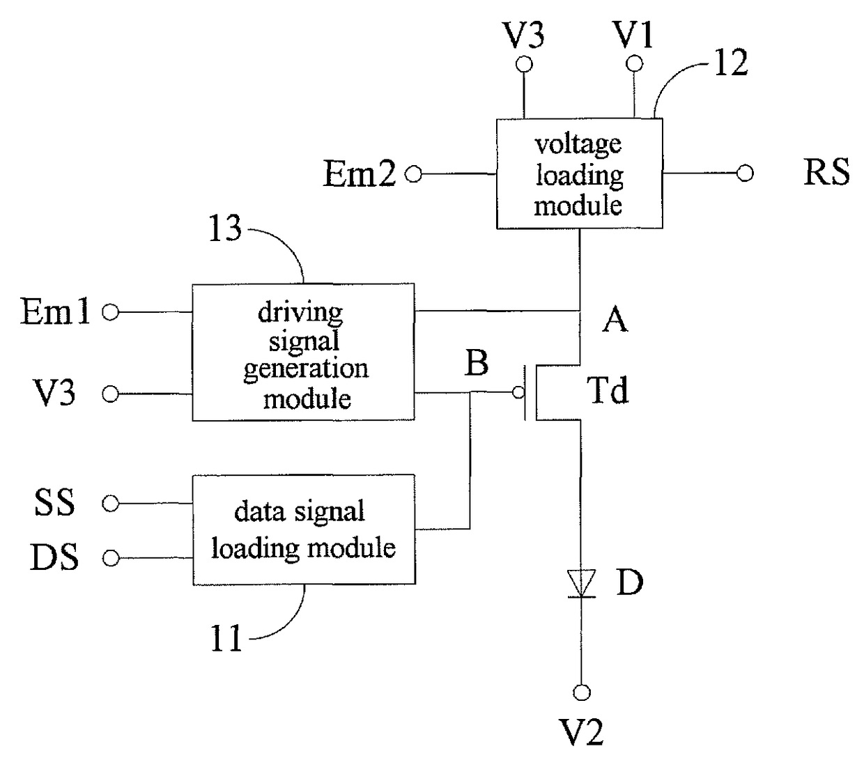
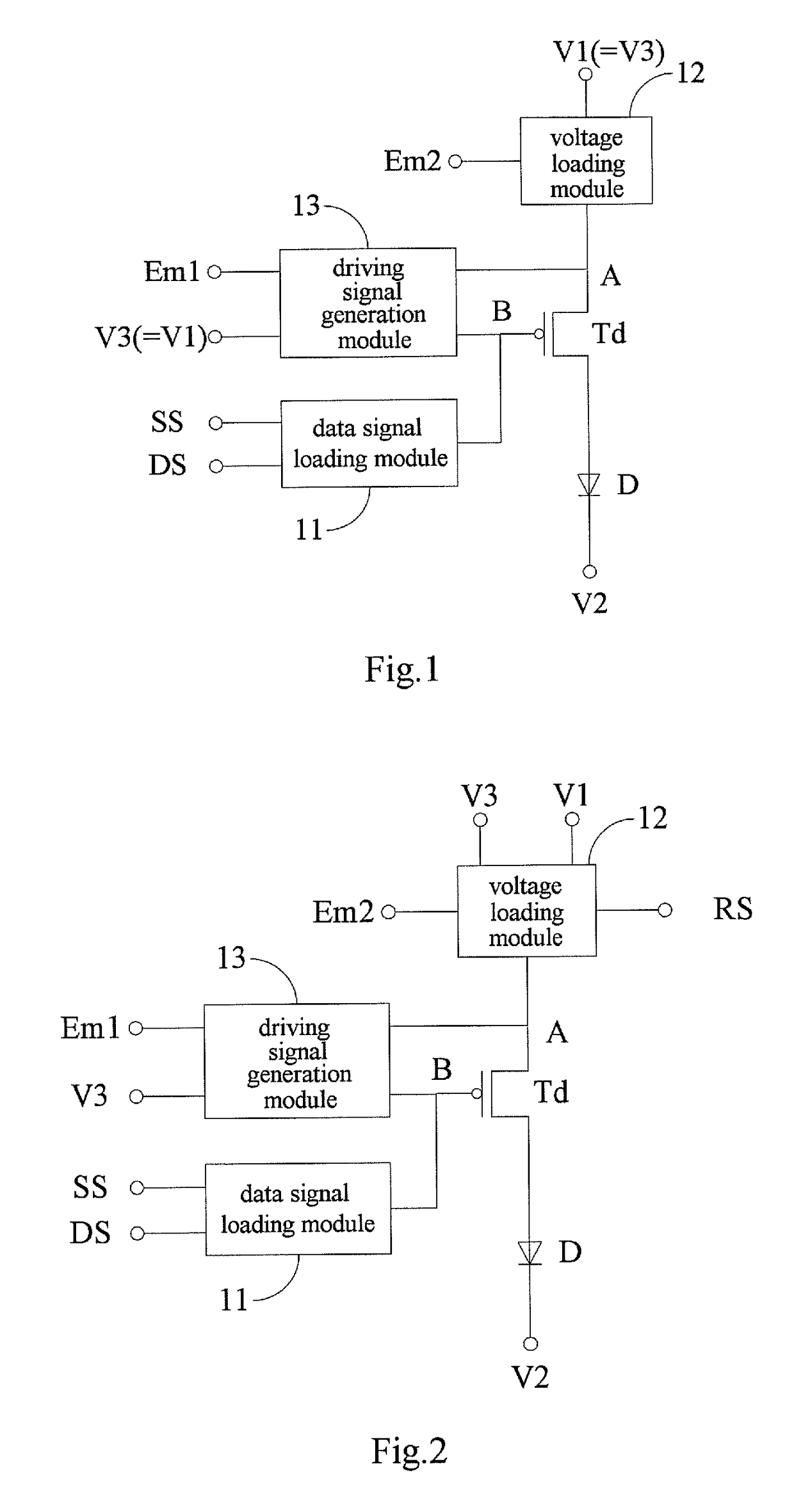
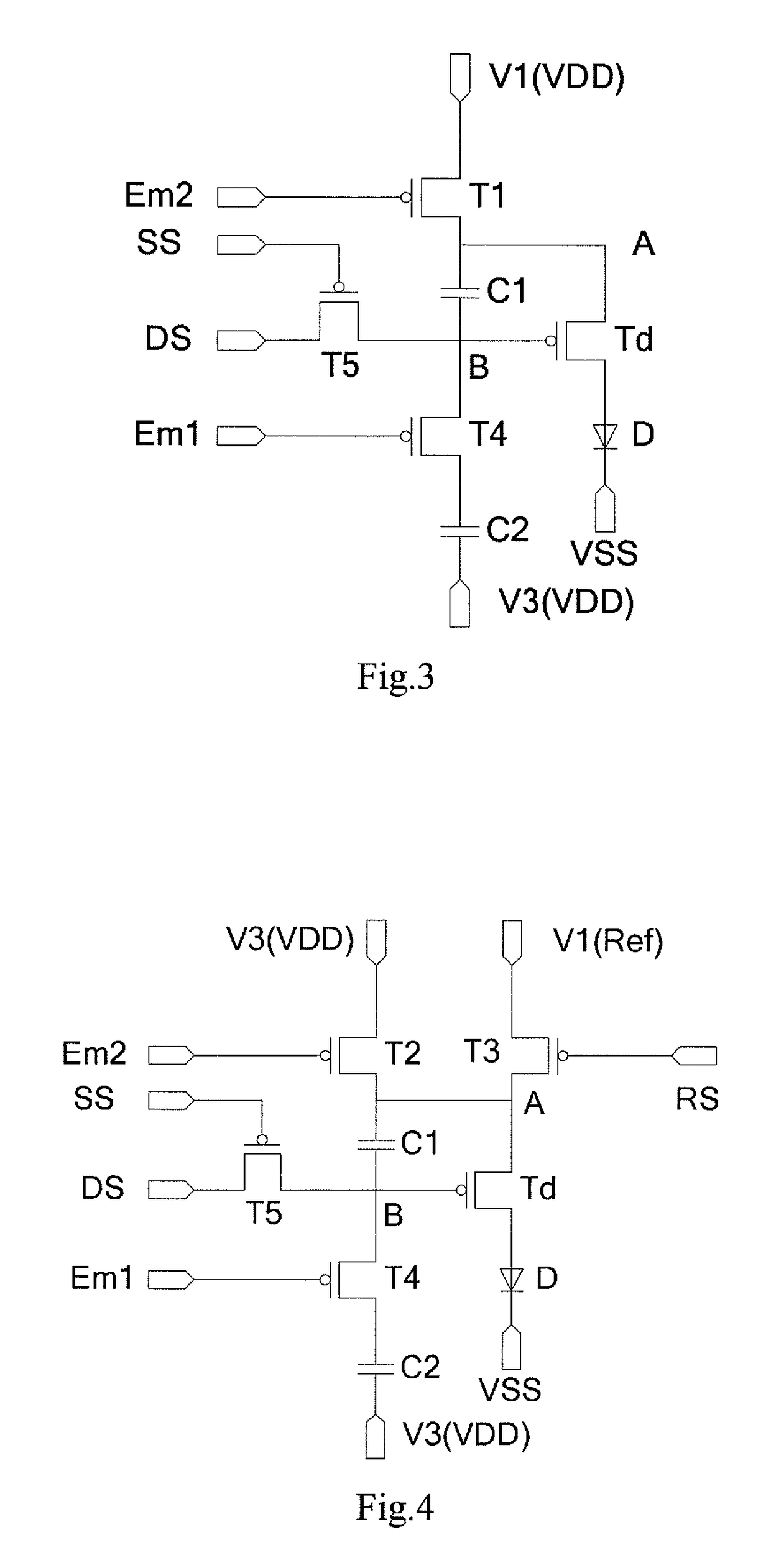
[0018]The transistor in the pixel compensation circuit provided by the embodiments of the present invention may be a p-type transistor and may also be an n-type transistor. When the transistor in the pixel compensation circuit is a p-type transistor, the turn-on signal is a low level signal, and the turn-off signal is a high level signal. When the transistor in the pixel compensation circuit is an n-type transistor, the turn-on signal is a high level signal, and the turn-off signal is a low level signal. Regardless of whether the transistor in the pixel compensation circuit is a p-type transistor or an n-type transistor, the circuit logic of the pixel compensation circuit is the same. Therefore, the following explanation is made only taking the case in which the transistor in the pixel compensation circuit is a p-type transistor as an example. The operational principle of the pixel compensation circuit consisting of the n-type transistor is similar to that of the pixel compensation ...


PUM


Abstract

The embodiments of the present invention provide a pixel compensation circuit, a display device and a driving method. The data signal loading module in the pixel compensation circuit loads the data signal to the gate of the driving transistor when the scanning signal is a turn-on signal. The voltage loading module loads the first voltage signal to the source of the driving transistor when the first luminescent signal and the scanning signal are both turn-on signals. The driving signal generation module is used for storing the signal of the source of the driving transistor, the signal of the gate of the driving transistor, the third voltage signal and the voltage signal inputted by the voltage loading module at that time; and is capable of generating a driving signal for driving the organic light-emitting diode to emit light.

Description

RELATED APPLICATIONS[0001]The present application is the U.S. national phase entry of PCT / CN2015 / 087620, with an international filling date of Aug. 20, 2015, which claims the benefit of Chinese Patent Application No. 201510106550.6, filed on Mar. 11, 2015, the entire disclosure of which are incorporated herein by referenceFIELD OF THE INVENTION[0002]The present invention relates to the display technical field, particularly to a pixel compensation circuit, display device and driving method.BACKGROUND OF THE INVENTION[0003]The active matrix organic light emitting diode display (AMOIED) has been widely used due to the advantages such as wide viewing angle, good color contrast effect, fast response speed and self illumination.[0004]AMOIED primarily employs low temperature poly-silicon as the driving layer to enable its pixel driving circuit. Compared to the general amorphous silicon technology, the low-temperature poly-silicon thin film transistor is characterized by higher mobility and...

Claims


Application Information

Patent Timeline
Patent Type & Authority Patents(United States)
IPC IPC(8): G09G3/3291G09G3/325G09G3/3233G09G3/3266G09G3/3225
CPCG09G3/3291G09G3/325G09G3/3233G09G3/3266G09G2320/0233G09G2300/0819G09G2300/0852G09G2300/0861G09G2310/08G09G2300/043
Inventor SUN, TUOMA, ZHANJIE
Owner BOE TECH GRP CO LTD
Features
  • R&D
  • Intellectual Property
  • Life Sciences
  • Materials
  • Tech Scout
  • Unparalleled Data Quality
  • Higher Quality Content
  • 60% Fewer Hallucinations
Learn More