
Semiconductor device

a technology of semiconductors and semiconductors, applied in the field of semiconductor devices, can solve problems such as information loss

Active Publication Date: 2017-10-31
MICRON TECH INC
View PDF17 Cites 85 Cited by
  • Summary
  • Abstract
  • Description
  • Claims
  • Application Information

AI Technical Summary

Benefits of technology

[0017]According to the present invention, access histories can be precisely analyzed by a small-scale circuit configuration.

Problems solved by technology

A dynamic random access memory (DRAM), which is a typical semiconductor memory device, stores information by charges accumulated in cell capacitors, and, therefore, the information is lost unless refresh operations are periodically carried out.

Method used


Image

  • Semiconductor device
  • Semiconductor device
  • Semiconductor device

Examples


first embodiment

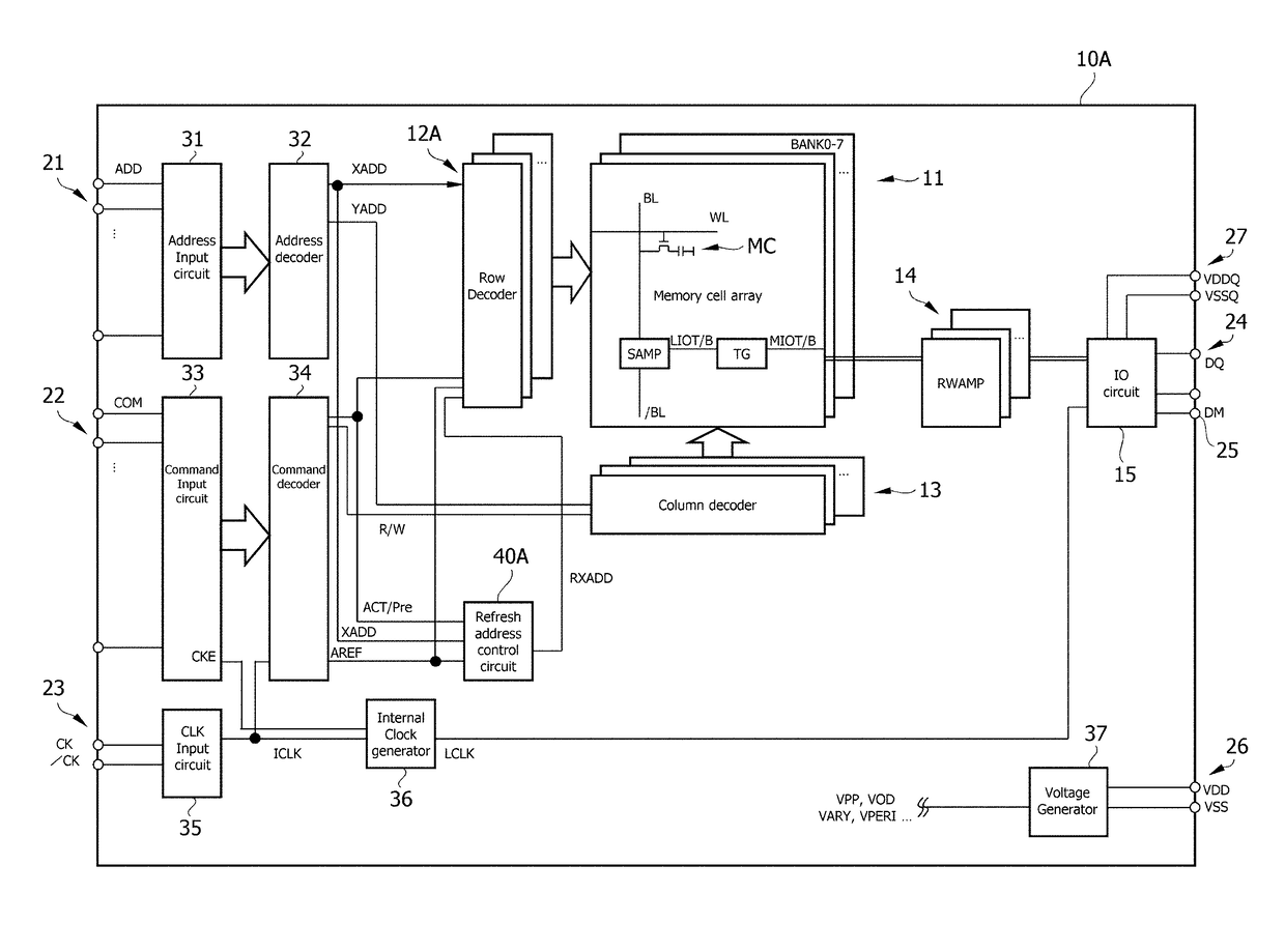
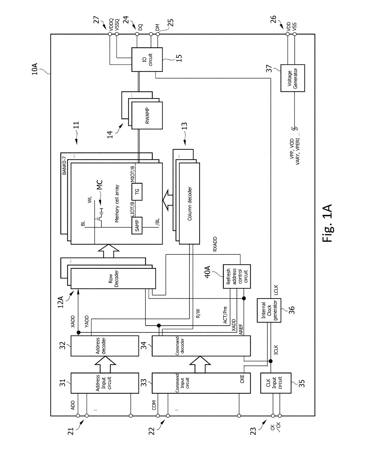
[0042]FIG. 1A is a block diagram showing an overall configuration of a semiconductor device 10A according to a first embodiment of the present invention.

[0043]The semiconductor device 10A according to the present embodiment is a synchronous DRAM (SDRAM) of, for example, a Double Data Rate 3 (DDR3) type integrated on a single semiconductor chip and has a memory cell array 11. The memory cell array 11 is provided with a plurality of word lines WL and a plurality of bit lines BL and has a configuration in which memory cells MC are disposed at the intersection points thereof. Selection of the word lines WL is carried out by a row decoder 12A, and selection of bit lines BL is carried out by a column decoder 13. The memory cell array 11, the row decoder 12A, the column decoder 13, and a read / write amplifier 14 are divided into eight banks BANK0 to BANK7.

[0044]Moreover, the semiconductor device 10A is provided with address terminals 21, command terminals 22, clock terminals 23, data termin...

second embodiment

[0084]FIG. 5A is a block diagram showing an overall configuration of a semiconductor device 10B according to a second embodiment of the present invention. In order to take measures against the Row Hammer problem, in the first embodiment of the present invention, the additional refresh operation (Row Hammer refresh) is carried out with respect to the adjacent address (victim address) of the row address selected by the refresh address control circuit 40A and having a high appearance frequency. On the other hand, in the second embodiment of the present invention described by FIG. 5A and thereafter, a row-copy operation is carried out with respect to the row address (aggressor address) selected by a refresh address control circuit 40B and having a high appearance frequency or with respect to an adjacent address (victim address) thereof

[0085]The semiconductor device 10B according to the present embodiment is different from the semiconductor device 10A according to the first embodiment in...


PUM


Abstract

A semiconductor device according to an aspect of the present invention has: a plurality of memory cells MC; a plurality of word lines WL each coupled to a corresponding one of the plurality of memory cells MC; and a control circuit that intermittently monitors accesses to the plurality of word lines WL, stores / erases some captured row-addresses in a first number of registers, and detects, by comparison with stored addresses, in response to a first number of accesses to one of the word lines WL in a first period of time. According to the present invention, access histories can be precisely analyzed by a small-scale circuit configuration, and measures against, for example, the Row Hammer problem, etc. can be taken.

Description

CROSS-REFERENCE TO RELATED APPLICATION(S)[0001]This application is based upon and claims the benefit of priority from Japanese Patent Application No. 2016-069963 filed on Mar. 31, 2016, the disclosure of which are incorporated herein in its entirety by reference.BACKGROUND[0002]The present invention relates to semiconductor devices and particularly relates to a semiconductor device that requires retention of information by refresh operations.TECHNICAL FIELD[0003]A dynamic random access memory (DRAM), which is a typical semiconductor memory device, stores information by charges accumulated in cell capacitors, and, therefore, the information is lost unless refresh operations are periodically carried out. Therefore, refresh commands indicating refresh operations are periodically issued from a control device, which controls a DRAM (see Patent Literature 1). The refresh commands are issued from the control device at a frequency that all the word lines are certainly refreshed one time in ...

Claims


Application Information

Patent Timeline
Patent Type & Authority Patents(United States)
IPC IPC(8): G11C11/406G11C11/408
CPCG11C11/4087G11C11/40611G11C29/846G11C11/406G11C29/72G11C29/783
Inventor ITO, YUTAKAHE, YUAN
Owner MICRON TECH INC
Learn More