Flyback diode and on-board power source device

a technology of power source device and flyback diode, which is applied in the direction of dynamo-electric converter control, semiconductor/solid-state device details, instruments, etc., can solve the problems of em not progressing in the solder layer bonding, the yield of obtaining sicsbd decreases, and the manufacturing cost of sicsbd increases, so as to facilitate the rate of branched current branching and heat generation

Active Publication Date: 2017-10-31
DENSO CORP
View PDF68 Cites 0 Cited by
  • Summary
  • Abstract
  • Description
  • Claims
  • Application Information

AI Technical Summary

Benefits of technology

[0008]Disclosed herein is a technique that enables slowing a progression rate of EM taking place in solder layers without enlarging a substrate area of a SiCSBD.
[0010]In a flyback diode, a large current may flow in some cases, and a small current may flow in other cases. For example, in a case of a flyback diode used in an on-board power source device to be mounted on an electric vehicle, a hybrid vehicle, or a fuel cell vehicle, a large current flows therein in a case where the vehicle accelerates rapidly, and a small current flows therein in a case where the vehicle runs in its normal state. In the case where a large current flows in the flyback diode, the flyback diode generates heat and comes to have a high temperature, and the EM easily progresses in this state. In the case where a small current flows in the flyback diode, a heat generating amount of the flyback diode is small, and the EM is less likely to progress.
[0013](i) During when the current flowing in the flyback diode is small, the heat generating amount of the flyback diode is small, and the flyback diode has a low temperature, the rate of the branched current branching to the SiPiND is low and most of the current flows in the SiCSBD. Even if most of the current flows in the SiCSBD, the EM does not progress in the solder layer bonded to the SiCSBD due to the flowing current being small and the temperature being low to begin with. Since most of the current flows in the SiCSBD, loss suppression is facilitated by the SiCSBD. As aforementioned, in the case of an on-board power source device, the aforementioned state takes place when a vehicle runs in a normal state. During the normal running state, the effect of loss suppression by the SiCSBD can be enjoyed. Consumption efficiency increases, and mileage until the next recharging or refueling can be increased.

Problems solved by technology

However, a SiC substrate contains a large number of crystal defects, and if the substrate area is increased, yield for obtaining the SiCSBD decreases and manufacturing cost of the SiCSBD is increased.
Even if most of the current flows in the SiCSBD, the EM does not progress in the solder layer bonded to the SiCSBD due to the flowing current being small and the temperature being low to begin with.

Method used


Image

  • Flyback diode and on-board power source device
  • Flyback diode and on-board power source device
  • Flyback diode and on-board power source device

Examples


first embodiment

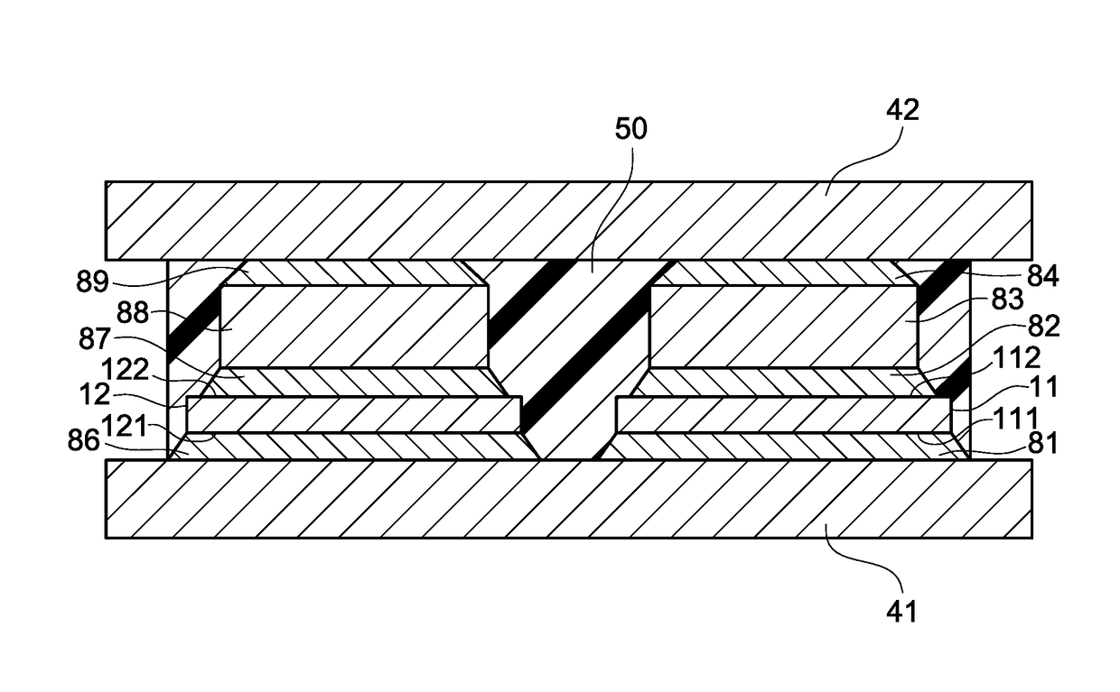
[0033]As shown in FIG. 1, an on-board power source device 1 of a first embodiment comprises a battery 31, a first capacitor 34, a converter 39, and a second capacitor 35. Power supplied from the battery 31 is output via the converter 39. The converter 39 boosts a voltage of the battery 31. The battery 31 is configured capable of recharging and discharging. This on-board power source device 1 is mounted for example on an electric vehicle, a hybrid vehicle, or a fuel cell vehicle and supplies power to a traction motor.

[0034]The converter 39 comprises a coil 32, a flyback diode 10 on an upper arm thereof, and a switching element 33 on a lower arm thereof. In the present embodiment, an IGBT (Insulated Gate Bipolar Transistor) is used as the switching element 33.

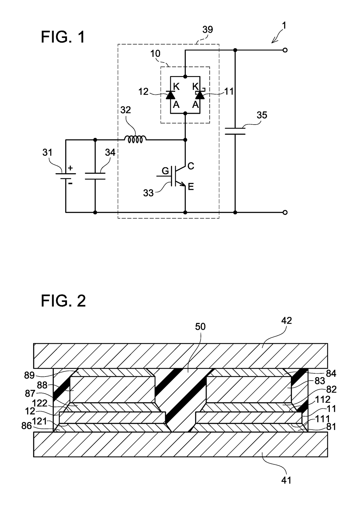
[0035]The flyback diode 10 comprises a Schottky-barrier diode (SiCSBD) 11 provided with a SiC substrate and a PiN diode (SiPiND) 12 provided with a Si substrate. The SiCSBD 11 and the SiPiND 12 are connected in parallel. The SiCS...

second embodiment

[0055]As shown in FIG. 4, an on-board power source device 101 of a second embodiment comprises a battery 31, a first capacitor 34, a converter 139, a second capacitor 35, a first inverter 91, and a second inverter 92. Power supplied from the battery 31 is input to the first inverter 91 and the second inverter 92 via the converter 139. The converter 139 boosts the battery 31.

[0056]The converter 139 comprises a coil 32, a first switching element 33, a flyback diode 136, a second switching element 137, and a flyback diode 10. In the present embodiment, a PiN diode provided with a Si substrate is used as the lower-arm flyback diode 136. Further, in the present embodiment, an IGBT is used as the upper-arm second switching element 137. Notably, the first switching element 33 has the same configuration as the switching element 33 of the above first embodiment.

[0057]The first switching element 33 and the flyback diode 136 are connected in anti-parallel. A cathode electrode of the flyback di...

example

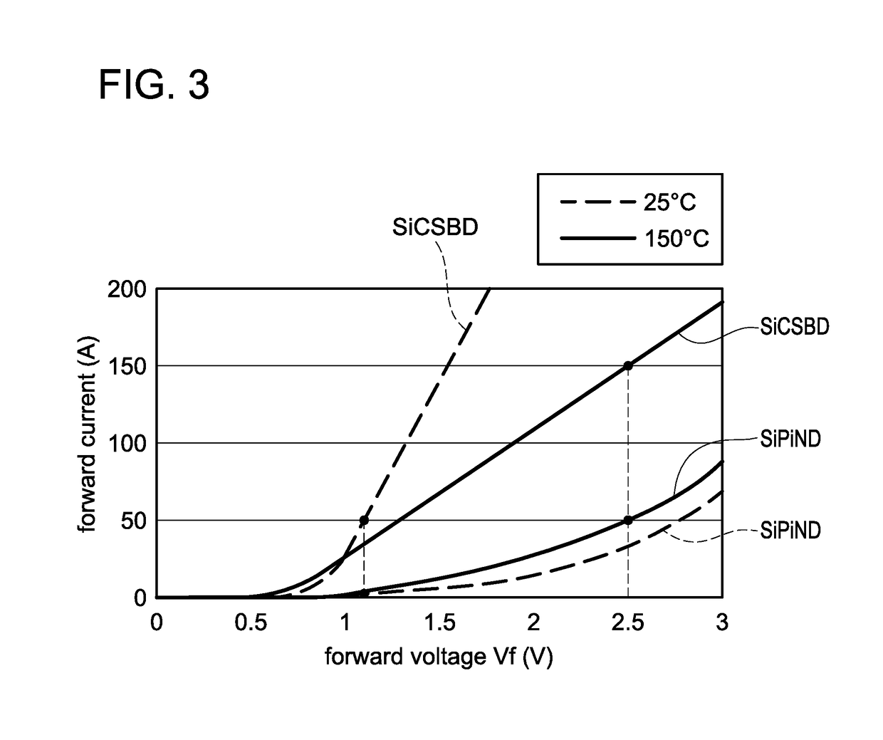
[0066]Next, one method of determining an area of the SiCSBD 11 and an area of the SiPiND 12 will be described. Firstly, a maximum rated current density by which the solder layers in the SiCSBD 11 can be used without a problem will be assumed as F (Amp / cm2=A / cm2). The maximum rated current density F can be obtained experimentally. For example, the maximum rated current density can be determined by considering a detaching rate of the solder layer 84, in which the EM is most likely to occur when a current flows in the SiCSBD 11. Further, the area of the SiCSBD 11 (area of an active region of the SiCSBD 11) will be assumed as E (cm2). In this case, a maximum current A (A) that flows in the SiCSBD 11 becomes A=F×E (A). Further, the forward voltage when the current A (A) flows in the SiCSBD 11 will be assumed as Vf1 (V).

[0067]On the other hand, a maximum rated current of the flyback diode 10 will be assumed as A+B (A). In this case, a current desired to flow in the SiPiND 12 of the flybac...


PUM


Abstract

A SiC Schottky-barrier diode and a SiPiN diode are connected in parallel. Due to a difference in their thermal properties, a relatively large current flows in the SiPiN diode at a high temperature in which electro migration progresses easily in a solder layer, and the progression of the electro migration is suppressed. At a low temperature in which the electro migration does not progress so much, only a relatively small current flows in the SiPiN diode, and a loss suppression by the SiC Schottky-barrier diode is achieved.

Description

CROSS-REFERENCE TO RELATED APPLICATION[0001]This application claims priority to Japanese Patent Application No. 2015-168251 filed on Aug. 27, 2015, the entire contents of which are hereby incorporated by reference into the present application.TECHNICAL FIELD[0002]The present application relates to a flyback diode and an on-board power source device.BACKGROUND ART[0003]A technique that connects a switching element and a diode in parallel, and utilizes the diode in a flyback diode is known (e.g. Japanese Patent Application Publication No. 2002-164503). When a current flowing in a coil (e.g., reactor or motor) is turned on or off by the switching element, electromotive force is generated in the coil. A current generated by the electromotive force flows in the flyback diode. Other than a PiN diode that uses a Si substrate (referred in this description as SiPiND), a Schottky-barrier diode that uses a SiC substrate (referred in this description as SiCSBD) is known. When a SiCSBD is used i...

Claims


Application Information

Patent Timeline
Patent Type & Authority Patents(United States)
IPC IPC(8): H02P1/00H02P27/00H02M7/537H02M7/46H01L25/07H01L23/492H02M3/155H02P27/06
CPCH02M7/537H01L23/492H01L25/072H02M7/46Y02B70/1483H01L2224/33H02M3/155H02P27/06Y02B70/10H01L2224/2612
Inventor SUGIURA, TOSHIKAZU
Owner DENSO CORP
Why Eureka
Try Eureka