
Eureka
For R&D, Eureka makes reading and utilizing patents & technical documents easy.
Eureka AIR
Designed for self-driven R&D workflows. Generate viable solutions, solve complex R&D challenges, empower your innovation with AI.

Eureka Materials
Designed for material experts only. Revolutionize your material R&D, from search, analyze, to developing new materials.

TechResearch
Generate reliable direction feasibility study reports for your R&D in just a few steps.

TechSeek
Discover and master advanced knowledge NOW. Basics, ideas, possibilities, all at once.

TechMind
As an expert in R&D Theories, TechMind can generates customized viable solutions instantly.

TechRisk
Analyze your overall solution with one click, know your potential R&D risks in advance.

TechMonitor
Get weekly tech updates, stay abreast of the latest tech innovations and key insights.
Semiconductor package and manufacturing method
- Summary
- Abstract
- Description
- Claims
- Application Information
AI Technical Summary
Benefits of technology
Problems solved by technology
Method used
Image

Examples
Embodiment Construction
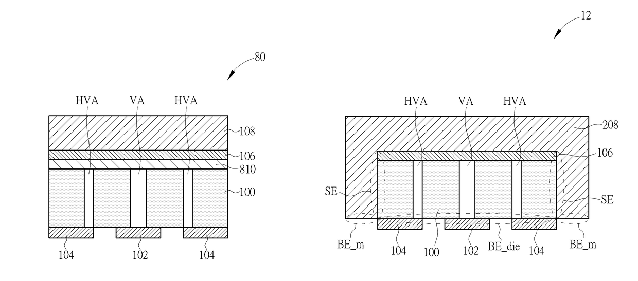
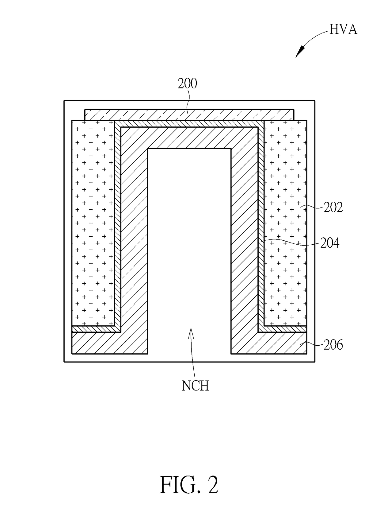
[0017]Please refer to FIG. 1, which is a schematic diagram of a sectional side view of a semiconductor package 10 according to an embodiment of the present invention. The semiconductor package 10 may be a radio frequency (RF) front end module (FEM) of a wireless communication device, and manufactured by a wafer level packaging (WLP) technology. The semiconductor package 10 comprises a die 100, a ground lead 102, signal leads 104, a buffer layer 106 and a molding portion 108. The die 100 may be a monolithic microwave integrated circuit (MMIC), manufacture by a Gallium Arsenide (GaAs) process, and applied in a high frequency or radio frequency (RF) application. The die 100 comprises hot vias HAV and vias VA for signal and ground connection. The hot vias HAV are configured to deliver an RF signal (or a DC signal) and the vias VA are used to provide grounding. The ground lead 102 and the signal leads 104 are formed directly under a back side of the die 100, which means that the ground l...
PUM
 Abstract
Description
Claims
Application Information
 - R&D Engineer
- R&D Manager
- IP Professional
- Industry Leading Data Capabilities
- Powerful AI technology
- Patent DNA Extraction
Browse by: Latest US Patents, China's latest patents, Technical Efficacy Thesaurus, Application Domain, Technology Topic, Popular Technical Reports.
© 2024 PatSnap. All rights reserved.Legal|Privacy policy|Modern Slavery Act Transparency Statement|Sitemap|About US| Contact US: help@patsnap.com