Collective substrate for resistor devices

a technology of resistor devices and substrates, which is applied in the direction of printed circuit non-printed electric components association, sustainable manufacturing/processing, and final product manufacturing, etc., can solve the problems of significant reduction of yield and significant reduction of yield, and achieve high yield

Active Publication Date: 2017-11-28
MURATA MFG CO LTD
View PDF9 Cites 4 Cited by
  • Summary
  • Abstract
  • Description
  • Claims
  • Application Information

AI Technical Summary

Benefits of technology

[0011]Preferred embodiments of the present invention provide a collective substrate for resistor devices enabling a high yield while avoiding upsizing of a to-be-cut-away region.
[0023]In accordance with various preferred embodiments of the present invention, a collective substrate for resistor devices is able to be provided that enables a high yield while avoiding upsizing of the to-be-cut-away region.

Problems solved by technology

In this case, if the substrate-type electronic device is of a considerably small size, the following problem arises.
Namely, even when to-be-product regions and to-be-cut-away regions are provided so that the to-be-product region and the to-be-cut-away region alternate with each other in a column or a row as disclosed in Japanese Patent Laying-Open Nos. 11-340002 and 2005-303199, connection between the electrode portion and the upper surface conductor which is connected to the resistive element may be difficult to make, or even this connection can be made, the to-be-cut-away region may be increased, resulting in significant reduction of the yield, namely the number of resistor devices produced from one collective substrate.
In this case, however, it is necessary to make the electrode portion accordingly large, resulting in significant reduction of the yield.

Method used


Image

  • Collective substrate for resistor devices
  • Collective substrate for resistor devices
  • Collective substrate for resistor devices

Examples


first preferred embodiment

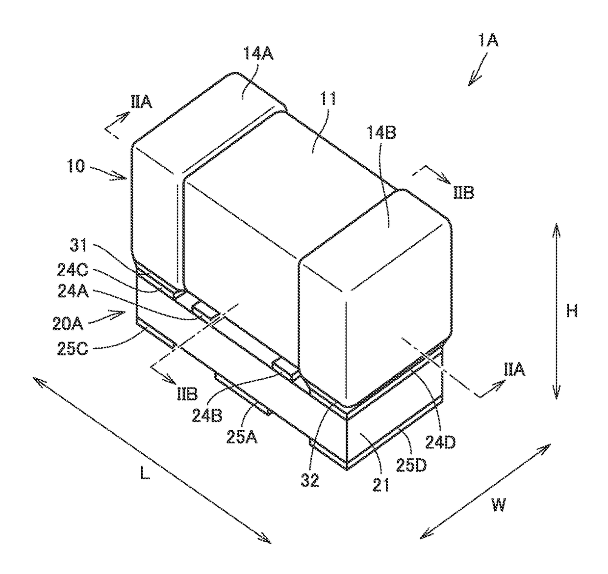
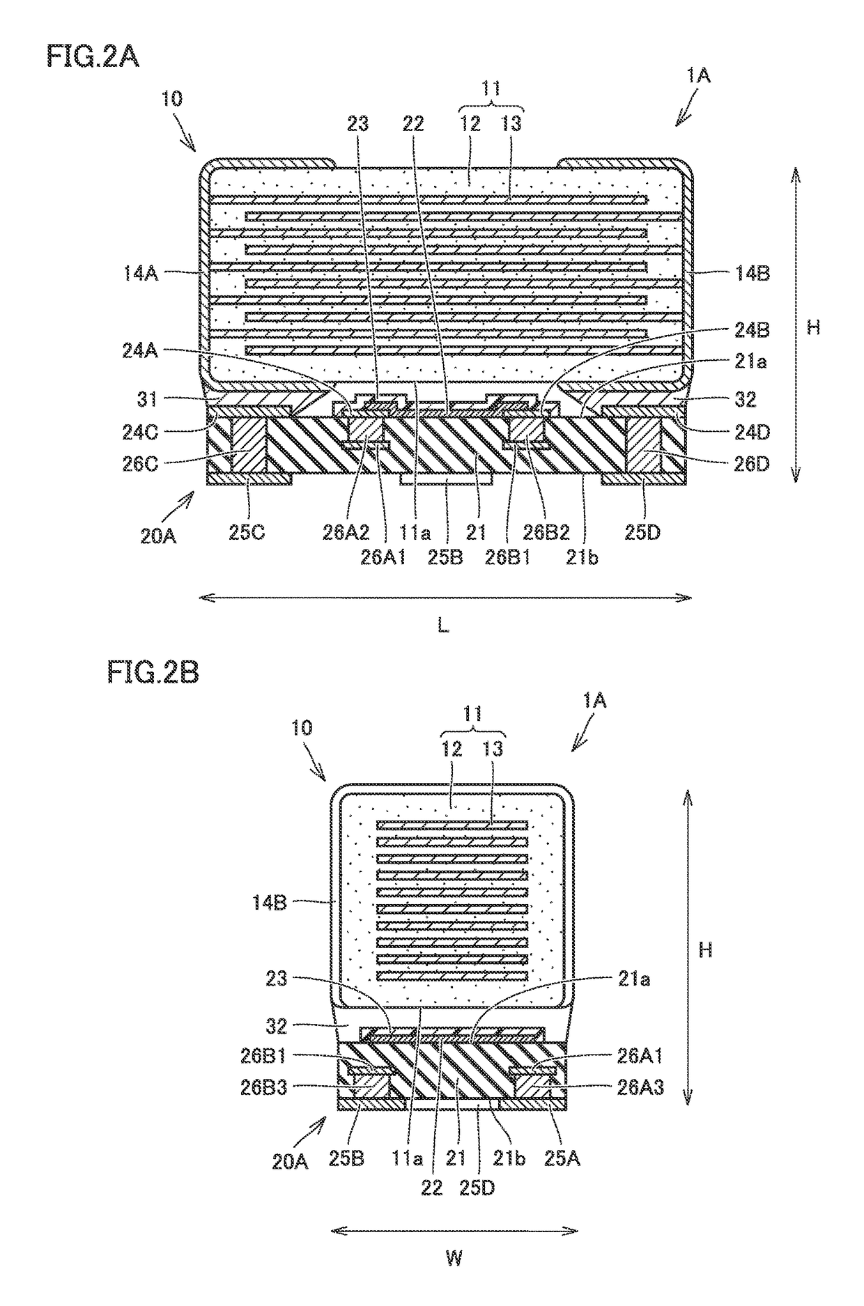
[0040]FIG. 1 is a schematic perspective view of a composite electronic component 1A including a resistor device 20A manufactured using a collective substrate 120A (see FIGS. 6 and 7) according to a first preferred embodiment of the present invention. FIGS. 2A and 2B are schematic cross-sectional views of composite electronic component 1A along a line IIA-IIA and a line IIB-IIB shown in FIG. 1, respectively. FIGS. 3A, 3B, and 3C are a schematic top view, a schematic cross-sectional view, and a schematic bottom view, respectively, of resistor device 20A shown in FIG. 1. FIG. 4 is a schematic perspective exploded view of composite electronic component 1A shown in FIG. 1.

[0041]Before providing a description of collective substrate 120A in the present preferred embodiment, a description will be given of resistor device 20A manufactured using collective substrate 120A, and of composite electronic component 1A including this resistor device 20A, with reference to FIGS. 1 to 4. It should be...

second preferred embodiment

[0122]FIG. 8 is a schematic top view of a collective substrate 120B according to a second preferred embodiment of the present invention, and FIG. 9 is a schematic top view showing, in an enlarged form, a unit region IX shown in FIG. 8. In the following, with reference to FIGS. 8 and 9, collective substrate 120B in the present preferred embodiment will be described. FIG. 8, like FIG. 6 as described above, shows a state of mother substrate 121 after the hardening of the protective film, and FIG. 9, like FIG. 7 as described above, shows a state of mother substrate 121 after baking of the resistive-element paste.

[0123]As shown in FIGS. 8 and 9, collective substrate 120B in the present preferred embodiment differs from collective substrate 120A in the first preferred embodiment in that collective substrate 120B does not include the substantially rectangular conductive patterns included in collective substrate 120A.

[0124]Specifically, as shown in FIG. 8, upper surface 121a of mother subst...

third preferred embodiment

[0135]FIG. 10 is a schematic perspective view of a composite electronic component 1B including a resistor device 20B manufactured using a collective substrate 120C (see FIGS. 13 and 14) according to the third preferred embodiment of the present invention. FIGS. 11A and 11B are schematic cross-sectional views of composite electronic component 1B along a line XIA-XIA and a line XIB-XIB shown in FIG. 10, respectively. FIGS. 12A and 12B are a schematic top view and a schematic bottom view, respectively, of resistor device 20B shown in FIG. 10.

[0136]Before a description of collective substrate 120C in the present preferred embodiment, a description will be given of resistor device 20B manufactured using collective substrate 120C, and of composite electronic component 1B including this resistor device 20B, with reference to FIGS. 10 to 12.

[0137]As shown in FIGS. 10 to 11B, composite electronic component 1B includes capacitor device 10 as a first electronic device and resistor device 20B a...


PUM

PropertyMeasurementUnit
heightaaaaaaaaaa
widthaaaaaaaaaa
lengthaaaaaaaaaa

Abstract

A collective substrate for resistor devices includes a base, a first conductive pattern in a to-be-product region and a to-be-cut-away region of the base, and a resistive element in the to-be-product region of the base. The to-be-cut-away region includes a first region adjacent to the to-be-product region in a first direction, and a second region adjacent to the to-be-product region in a second direction. The first conductive pattern includes a first terminal portion connected to the resistive element and disposed in the to-be-product region, a first electrode portion disposed in the first region and larger in area than the first terminal portion, and a first interconnect portion extended from the first terminal portion toward the second region to be connected to the first electrode portion.

Description

CROSS REFERENCE TO RELATED APPLICATIONS[0001]This application claims the benefit of priority to Japanese Patent Application 2015-166914 filed Aug. 26, 2015, the entire contents of this application are hereby incorporated herein by reference.BACKGROUND OF THE INVENTION1. Field of the Invention[0002]The present invention relates to a collective substrate for resistor devices (hereinafter also referred to simply as a collective substrate). The collective substrate is a work in process in which a plurality of resistor devices to be included in composite electronic components are manufactured together.2. Description of the Related Art[0003]Inventions for a composite electronic component made up of a plurality of electronic devices have been proposed in terms of integration of electronic devices at a high density.[0004]For example, Japanese Patent Laying-Open No. 6-283301 discloses a composite electronic component into which a plurality of electronic devices that are identical in shape an...

Claims


Application Information

Patent Timeline
Patent Type & Authority Patents(United States)
IPC IPC(8): H05K7/00H05K1/02H01C7/00H01G4/248H01G4/12H01G4/30H05K1/18H01C1/01
CPCH05K1/181H01C1/01H01C7/008H01G4/12H01G4/248H05K1/0296H01G4/30H05K2201/10022H05K2201/0909H05K2201/1003H05K2201/10015H01C7/001H01G4/40H01C1/014H01C1/142H01C1/148H01C7/18H01G2/065H01G4/232H05K2201/10515H05K2201/1053H05K2201/10636Y02P70/50H01C1/012H01C17/06
Inventor HATTORI, KAZUOFUJIMOTO, ISAMUKUROIWA, SHINICHIRO
Owner MURATA MFG CO LTD
Why Eureka
Try Eureka