Device and method for proximity sensing with force imaging

a technology of force imaging and proximity sensing, applied in the field of electronic devices, can solve the problems of increasing the cost and complexity of the presently known force enabled input device, and achieve the effects of enhancing the variable capacitance, facilitating the improvement of device usability, and improving user interface functionality

Active Publication Date: 2017-12-12
SYNAPTICS INC
View PDF37 Cites 16 Cited by
  • Summary
  • Abstract
  • Description
  • Claims
  • Application Information

AI Technical Summary

Benefits of technology

[0005]Embodiments of the present invention provide a device and method that facilitates improved device usability. The device and method provide improved user interface functionality by strategically arranging both the touch sensing and force sensing electrodes on a single flexible substrate (or laminate), with a compliant component separating the substrate from a conductive layer. In response to applied force, the touch and force electrodes move towards the conductive layer, changing the capacitance between the force electrodes and the conductive layer in a detectable way. Other embodiments include an additional floating electrode layer disposed between the force electrodes and the conductive layer to enhance the variable capacitance and, hence, the pressure sensitivity, of the force sensing electrodes. Displaceable air gaps may also be disposed between the force pixels and the conductive substrate and configured to increase the electrical permittivity and, hence, the force response, of the force pixels responsive to applied pressure.

Problems solved by technology

However, in presently known force / proximity input devices the various touch and force electrodes are disposed on two or more substrates, thereby increasing the cost and complexity of presently known force enabled input devices.

Method used


Image

  • Device and method for proximity sensing with force imaging
  • Device and method for proximity sensing with force imaging
  • Device and method for proximity sensing with force imaging

Examples


Embodiment Construction

[0013]The following detailed description is merely exemplary in nature and is not intended to limit the invention or the application and uses of the invention. Furthermore, there is no intention to be bound by any expressed or implied theory presented in the preceding technical field, background, brief summary or the following detailed description.

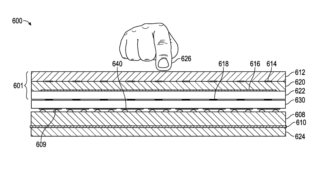
[0014]Various embodiments of the present invention provide input devices and methods that facilitate simple construction, reduced cost, and enhanced force sensing capability resulting in improved usability. Device cost and complexity may be reduced by disposing three electrode arrays (touch receiver, force receiver, and common transmitter) on a single substrate or laminate. In response to applied pressure, the pliable electrode substrate deforms in the vicinity of the applied force, such that all three electrode arrays move without appreciable relative motion among the respective arrays. That is, the touch pixels and force pixels move in u...


PUM


Abstract

Methods, systems and devices are described for operating an electronic system which includes a pliable component having an input surface, a first array of sensor electrodes, a second array of sensor electrodes, and a third array of sensor electrodes. The input device also includes a conductive substrate spaced apart from the pliable component and a compliant component disposed between the pliable component and the conductive substrate. In response to pressure applied by an input object to the input surface, the pliable component and the first, second, and third arrays of sensor electrodes locally deform and the compliant component locally compresses such that a spacing between the conductive substrate and at least one electrode from each of the first, second, and third arrays decreases.

Description

TECHNICAL FIELD[0001]This invention generally relates to electronic devices, and more specifically relates to sensor devices and using sensor devices for producing user interface inputs.BACKGROUND[0002]Input devices including proximity sensor devices (also commonly called touchpads or touch sensor devices) are widely used in a variety of electronic systems. A proximity sensor device typically includes a sensing region, often demarked by a surface, in which the proximity sensor device determines the presence, location and / or motion of one or more input objects. Proximity sensor devices may be used to provide interfaces for the electronic system. For example, proximity sensor devices are often used as input devices for larger computing systems (such as opaque touchpads integrated in, or peripheral to, notebook or desktop computers). Proximity sensor devices are also often used in smaller computing systems (such as touch screens integrated in cellular phones).[0003]The proximity sensor...

Claims


Application Information

Patent Timeline
Patent Type & Authority Patents(United States)
IPC IPC(8): G06F3/045G06F3/044G06F3/041
CPCG06F3/044G06F3/0414G06F2203/04111G06F2203/04108G06F2203/04105G06F3/0445G06F3/0447
Inventor SCHEDIWY, RICHARD R.KALLASSI, PASCALE EL
Owner SYNAPTICS INC
Why Eureka
Try Eureka