Nitride semiconductor light-emitting device with periodic gain active layers

a technology of active layers and nitride semiconductors, which is applied in semiconductor devices, semiconductor lasers, laser details, etc., can solve the problems of reducing the performance of nitride semiconductor light-emitting devices

Active Publication Date: 2017-12-19
MEIJO UNIVERSITY +1
View PDF10 Cites 0 Cited by
  • Summary
  • Abstract
  • Description
  • Claims
  • Application Information

AI Technical Summary

Benefits of technology

[0010]In the first one of the above-described nitride semiconductor light-emitting devices, the active layer disposed at the p-type semiconductor layer side has a larger light emission intensity than the active layer disposed at the n-type semiconductor layer side. In the second nitride semiconductor light-emitting device, an amount of positive holes and electrons injected into the active layer disposed at the p-type semiconductor layer side is larger than an amount of positive holes and electrons injected into the active layer disposed at the n-type semiconductor layer side. In each nitride semiconductor light-emitting device, a concentration of Mg as the p-type impurity doped into the interlayer can be reduced to a low level. This can suppress a reduction in the crystal quality of the active layer disposed at the p-type semiconductor layer side and accordingly a reduction in the light emission intensity of the nitride semiconductor light-emitting device with the periodic gain active layers. Accordingly, the device can successfully emit light.
[0011]In each of the above-described devices, Mg as a p-type impurity doped into the interlayer may have a concentration of not more than 5×1018 cm−3. In this case, each device can suppress reduction in the light emission intensity relative to the current density.
[0013]In each one of the above-described devices, two active layers may be provided and have respective light emission wavelengths equal to each other. In this case, the resonator in each device can successfully resonate by a gain of the active layer.

Problems solved by technology

As a result, there is a possibility that the performance of the nitride semiconductor light-emitting device would be reduced.

Method used


Image

  • Nitride semiconductor light-emitting device with periodic gain active layers
  • Nitride semiconductor light-emitting device with periodic gain active layers
  • Nitride semiconductor light-emitting device with periodic gain active layers

Examples


first embodiment

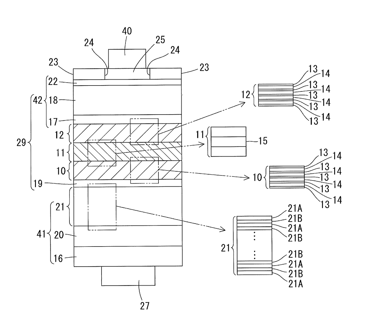
[0023]A nitride semiconductor light-emitting device with periodic gain active layers according to a first embodiment includes a first active layer (corresponding to an active layer disposed at an n-type semiconductor layer side) and a second active layer (corresponding to an active layer disposed at a p-type semiconductor layer side) into both of which carriers (electrons and holes (positive holes)) need to be injected evenly. In more detail, in order that carriers may evenly be injected into the first and second active layers, a suitable amount of p-type impurity needs to be doped into an interlayer provided between the first and second active layers thereby to enhance injection of holes into the first active layer. Holes have a lower mobility and a larger effective mass than electrons. Furthermore, the first active layer is disposed with the second active layer and the interlayer being interposed between the p-type semiconductor layer serving as a hole-supply source and the first ...


PUM


Abstract

A nitride semiconductor light-emitting device with periodic gain active layers includes an n-type semiconductor layer, a p-type semiconductor layer and a resonator. The device further includes a plurality of active layers disposed between the n-type and p-type semiconductor layers so as to correspond to a peak intensity position of light existing in the resonator and at least one interlayer disposed between the active layers. The active layer disposed at the p-type semiconductor layer side has a larger light emission intensity than the active layer disposed at the n-type semiconductor layer side.

Description

CROSS-REFERENCE TO RELATED APPLICATIONS[0001]This application is based upon and claims the benefit of priority from the prior Japanese Patent Application No. 2014-245909 filed on Dec. 4, 2014, the entire contents of which are incorporated herein by reference.BACKGROUND[0002]1. Technical Field[0003]The present disclosure relates to a nitride semiconductor light-emitting device with periodic gain active layers.[0004]2. Related Art[0005]There have conventionally been provided nitride semiconductor light-emitting devices with periodic gain active layers. One of these conventional nitride semiconductor light-emitting devices includes a first active layer, a second active layer and an interlayer provided between the first and second active layers. In the device, furthermore, an amount of magnesium (Mg) as a p-type impurity doped into the interlayer is adjusted so that carriers (electrons and holes (positive holes)) are supplied to the first and second active layers in a balanced manner. H...

Claims


Application Information

Patent Timeline
Patent Type & Authority Patents(United States)
IPC IPC(8): H01L29/06H01L31/00H01L33/06H01L33/10H01S5/00
CPCH01L33/06H01S5/00H01L33/105H01S5/1096H01S5/18341H01S5/18369H01S5/18383H01S5/34333H01S5/3063H01S2304/04H01S5/04253H01S5/04254
Inventor MATSUI, KENJOTAKEUCHI, TETSUYAIWAYA, MOTOAKIAKASAKI, ISAMUAKAGI, TAKANOBUIWAYAMA, SHO
Owner MEIJO UNIVERSITY
Why Eureka
Try Eureka