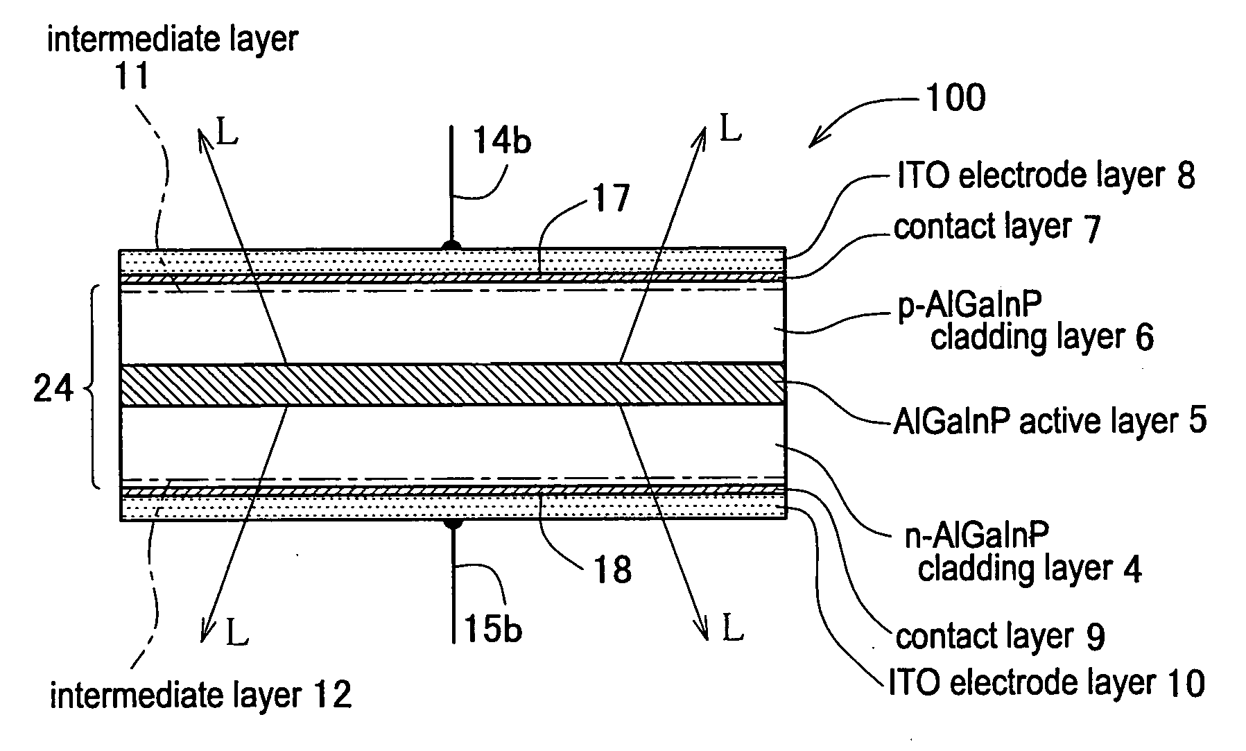
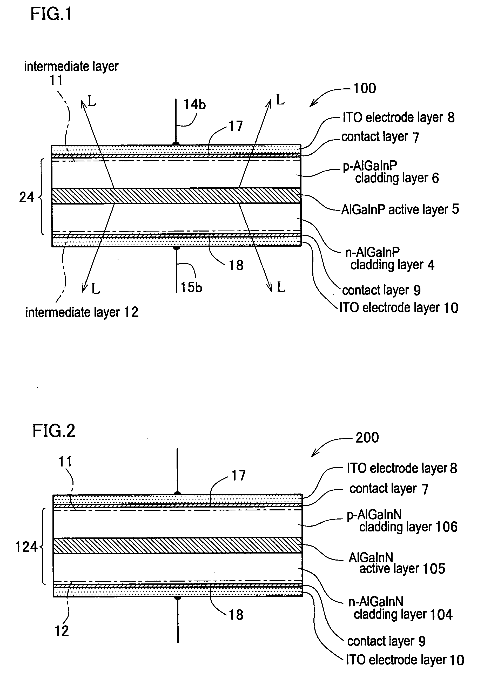
[0010] The aforementioned light-emitting layer section can realize an extremely high
light emission efficiency, because holes and electrons injected in the narrow
active layer are confined and can efficiently recombine, due to energy barriers ascribable to difference in the
band gap between the
active layer and the cladding layer formed on both sides thereof. It is also made possible to realize a wide range of emission
wavelength from green to red regions (with a peak emission
wavelength of 520 nm to 670 nm, both ends inclusive), through compositional adjustment of the
active layer composed of AlGaInP. In the method of fabricating a light-emitting device of this invention, the GaAs layer is formed on the light-emitting layer section composed of AlGaInP, and the ITO transparent electrode layer is formed so as to contact with the GaAs layer. The light-emitting layer section is typically composed of a III-V
compound semiconductor, and can typically be formed by the publicly-known MOVPE process, together with the GaAs layer formed thereon (where,
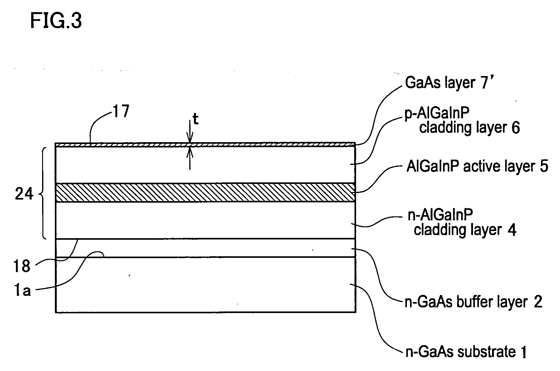
insertion of any other lattice-matched layer permissible). The GaAs layer can very readily be lattice-matched with the AlGaInP light-emitting layer section, and can form a uniform and highly continuous film as compared with the case of direct epitaxial growth of InGaAs disclosed in Japanese Laid-Open Patent Publication “Tokkaihei” No. 1-225178.
[0011] The ITO transparent electrode layer is then formed on the GaAs layer, and the stack is annealed so as to allow In to diffuse from the ITO transparent electrode layer into the GaAs layer, to thereby form the contact layer. The contact layer composed of In-containing GaAs thus obtained through the annealing will never have an excessive In content, and can effectively prevent quality degradation such as lowering in the
emission intensity due to lattice mismatching with the light-emitting layer section. The lattice matching between the GaAs layer and the light-emitting layer section becomes particularly desirable when the light-emitting layer section is composed of (AlxGa1-x)yIn1-yP (where, 0≦x≦1, 0.45≦y≦0.55), so that it can be said desirable to form the light-emitting layer section (cladding layer or active layer) while adjusting
alloy composition y within the above range.
[0015] ITO is an
indium oxide film doped with
tin oxide, and adjustment of
tin oxide content thereof to 1% by
mass to 9% by
mass (
indium oxide content to 91% by
mass to 99% by mass) can suppress resistivity of the electrode layer to as low enough as 5×10⁻⁴ Ω·cm. Formation of this sort of ITO transparent electrode layer on the GaAs layer, and by further annealing it within an appropriate temperature range makes it possible to readily form the contact layer having the above-described desirable In concentration. The annealing is also successful in further reducing the resistivity of the ITO transparent electrode layer. The annealing is preferably carried out within a temperature range lower than that described in the Japanese Laid-Open Patent Publication “Tokkaihei” No. 1-225178, more specifically in a range from 600° C. to 750° C. The annealing temperature exceeding 750° C. results in a too large
diffusion rate of In into the GaAs layer, and tends to make the In concentration in the contact layer excessive. This also results in saturation of the In concentration and makes it difficult to obtain the In
concentration gradient in the thickness-wise direction in the contact layer. The both consequently worsen the lattice matching between the contact layer and the light-emitting layer section. An excessive proceeding of the In
diffusion into the GaAs layer causes In depletion in the ITO transparent electrode layer at around the contact portion with the contact layer, and inevitably results in increase in the resistivity of the electrode. Furthermore, the above-described excessively high annealing temperature makes
oxygen in ITO diffuse into the GaAs layer and promote oxidation, and thereby makes the series resistance of the device more likely to increase. Both cases raise nonconformity in that the light-emitting device cannot be driven at an appropriate
voltage. An extremely high annealing temperature may sometimes worsen the resistivity of the ITO transparent electrode layer, against expectation. On the other hand, the annealing temperature less than 650° C. excessively lowers the diffusion rate of In into the GaAs layer, and needs an extremely long time for obtaining the contact layer lowered in the
contact resistance to a satisfactory degree, and this considerably lowers efficiency in the fabrication.
[0017] The ITO transparent electrode layer can be formed so as to cover the entire surface of the light-emitting layer section. This configuration makes the ITO transparent electrode layer have a function of current spreading layer, and consequently makes it possible to get rid of a conventional thick current spreading layer composed of a
compound semiconductor, or makes it possible to largely reduce the thickness if it is daringly formed. This contributes to the cost reduction through simplification of the process, and is very beneficial in terms of industrial application. On the other hand, the thickness of the contact layer may not so necessarily be large so far as it is thick enough to form
ohmic contact. More specifically, it is all enough to secure the thickness so that the
compound semiconductor composing the contact layer will never show a
band gap energy different from that of the
bulk crystal due to
thinning of the layer, and a thickness of 0.001 μm or around will be sufficient when InxGa1-xAs is used. On the other hand, excessive increase in the thickness of the contact layer composed of InxGa1-xAs results in increase in light absorption by the contact layer, and lowers the light extraction efficiency. The thickness is therefore preferably adjusted to 0.02 μm or below. Making the contact layer as a
thin layer of 0.001 μm to 0.02 μm thick is also effective in terms of moderating influences of the lattice mismatching.
[0020] On the contrary, there is no need of considering the carrier dam-up effect by the barrier when the ITO transparent electrode layer is used, because the ITO transparent electrode layer per se has an extremely large current spreading ability. What is better, adoption of the ITO transparent electrode layer is successful in considerably increasing area of the light extraction region as compared with that for the case where the metal electrode is used.
Insertion, between the contact layer and the cladding layer, of the intermediate layer having a
band gap energy intermediate of those of the contact layer and the cladding layer, as shown in FIG. 11, reduces band edge discontinuity values between the contact layer and the intermediate layer, and between the intermediate layer and the cladding layer, respectively, and thereby the individual barrier heights ΔE formed therebetween become small. This is consequently successful in moderating the series resistance, and in achieving a sufficiently large light emitting intensity at a low drive voltage.

