Method of manufacturing a semiconductor device

a semiconductor device and manufacturing method technology, applied in semiconductor devices, diodes, radiation controlled devices, etc., can solve the problems of limited integration of on-glass (substrat) circuits to reduce the total number of external drivers or introduce high-performance data schemes, and achieve the effect of preventing electrical damag

Active Publication Date: 2017-12-26
DPIX
View PDF2 Cites 2 Cited by
  • Summary
  • Abstract
  • Description
  • Claims
  • Application Information

AI Technical Summary

Benefits of technology

[0007]Overshadowing the technical situation described above is an overall trend in flat panel imaging to reduce overall system cost and / or increase acquisition speed (i.e. increased frame rate.)
[0011]It is also important to note that the partially formed image sensor device must be both mechanically and electrically protected so that it can be shipped to the second manufacturing facility without appreciable loss of product due to mechanical damage in transit or electrical damage due to overvoltage stress from static electricity. The partially formed image sensor is completely covered by a passivation or other type of layer that both adds mechanical support and prevents electrical damage. The passivation layer is removed at the second manufacturing facility and the manufacturing process resumes with the same or a different semiconductor process. Finally, the image sensor device is again passivated.

Problems solved by technology

Furthermore, the integration of on-glass (substrate) circuits to reduce the total number of external driver or to introduce high performance data schemes is limited due to the intrinsic threshold bias instability (Vt shift) of amorphous Silicon as well as the low electron mobility.

Method used


Image

  • Method of manufacturing a semiconductor device
  • Method of manufacturing a semiconductor device
  • Method of manufacturing a semiconductor device

Examples


Embodiment Construction

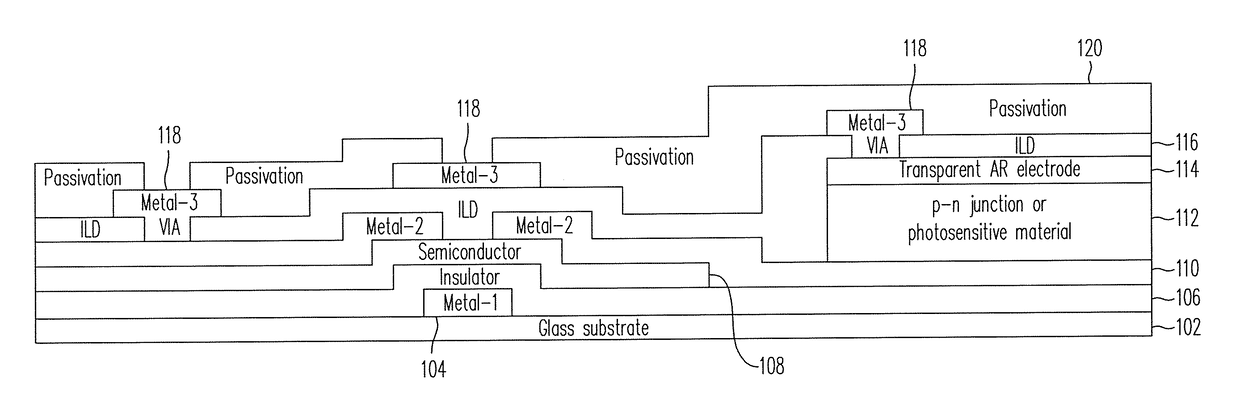
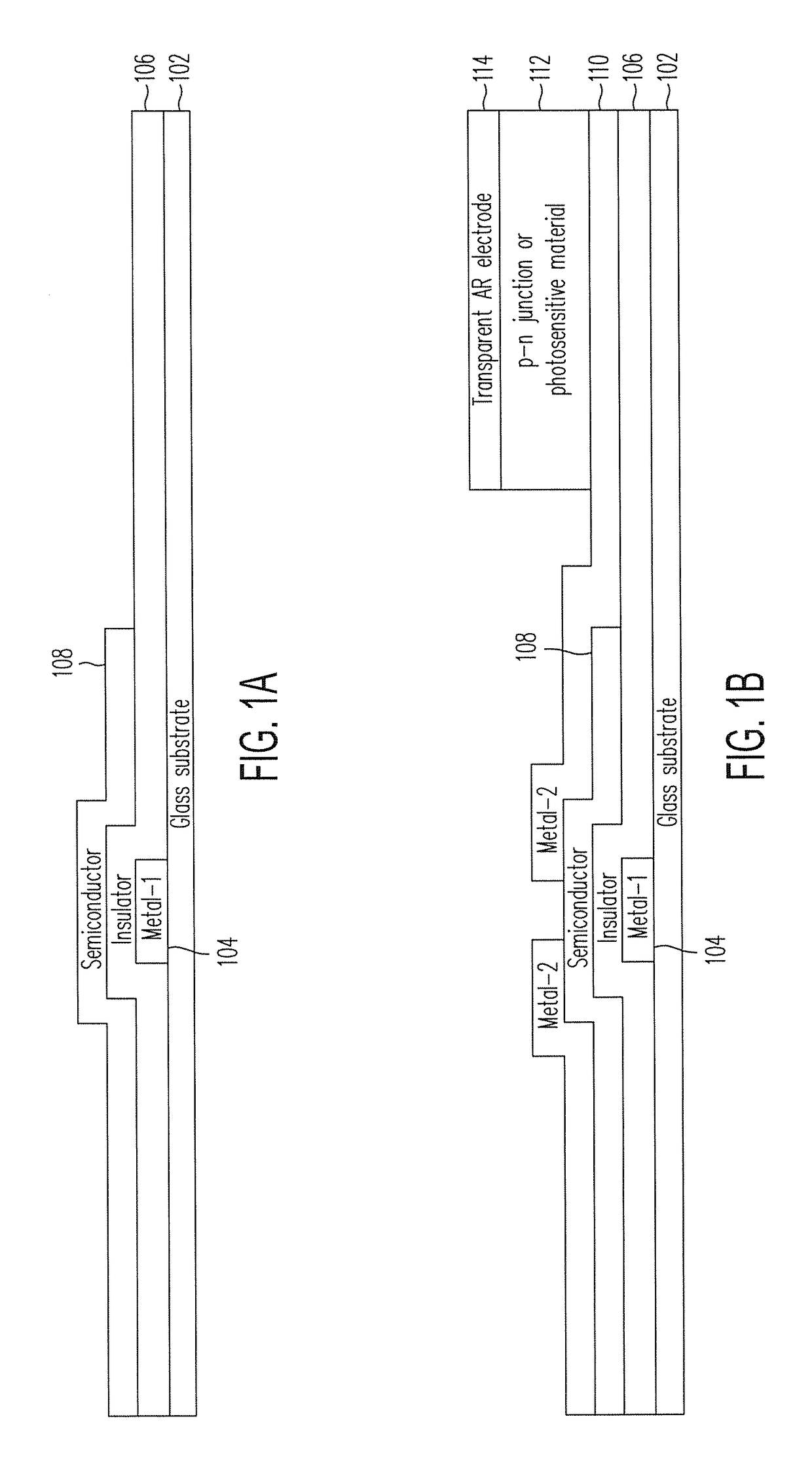
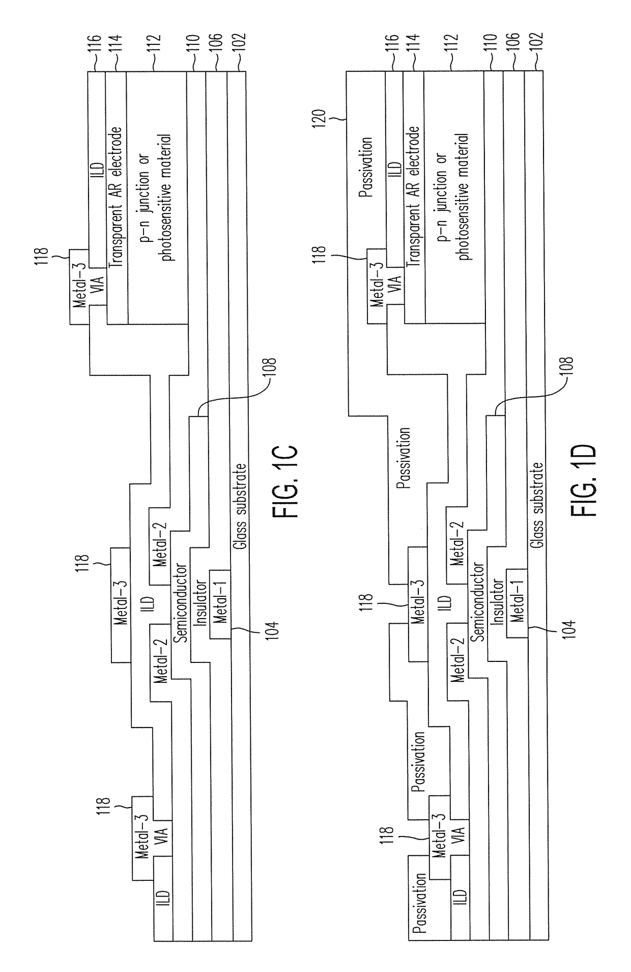
[0025]A manufacturing process for an image sensor device performed in a single manufacturing facility is illustrated with respect to FIGS. 1A-1D.

[0026]FIG. 1A illustrates the first process steps used to build TFT (Thin-Film Transistor) devices. These devices are field-effect transistors (FETs) that can be either a Metal-Insulator-Semiconductor (MIS) or Metal-Oxide-Semiconductor (MOS) structure. FIG. 1A illustrates a bottom-gate TFT process flow, but a top-gate process flow can be used as well. FIG. 1A illustrates a glass substrate 102, a first metal layer 104 that has been etched to form a gate, an insulator layer 106, and a semiconductor layer 108.

[0027]FIG. 1B illustrates the second process steps that are used to build photo-sensitive devices. These devices could be photodiodes formed with p-n junctions or photosensitive compounds. The electrode facing incident photons is made of a transparent and / or anti-reflective (AR) material. In addition to the previously described layers, FI...


PUM


Abstract

A method of manufacturing an image sensor device includes, in a first manufacturing facility, forming a first set of patterned silicon, metal, and insulating layers on a glass substrate, forming an electrical and mechanical protection layer over the first set of patterned silicon, metal, and insulating layers, and, in a second manufacturing facility, removing the electrical and mechanical protection layer, forming a second set of patterned silicon, metal, and insulating layers over the first set of patterned silicon, metal, and insulating layers, forming a plurality of photosensors in communication with at least the second set of patterned silicon, metal, and insulating layers to form an unpassivated image sensor device, and forming a passivation layer over the unpassivated image sensor device. The materials used in the first set of layers and second set of layers can be completely or partially different.

Description

RELATED APPLICATIONS[0001]The present application relates to and claims priority of U.S. provisional patent application (“Provisional Application”), Ser. No. 62 / 284,209, filed on Sep. 23, 2015. The disclosure of the Provisional Application is hereby incorporated by reference in its entirety.BACKGROUND OF THE INVENTION[0002]1. Field of the Invention[0003]The present invention generally relates to image sensor devices, and, more particularly, to a method for manufacturing the image sensor devices.[0004]2. Relevant Background[0005]Image sensor devices are known in the art and are typically manufactured at a single manufacturing facility. A subset of image sensor devices includes a glass substrate and can be used, for example, as a flat panel imager for use in X-ray imaging (digital radiography). This type of image sensor device is also typically manufactured at a single manufacturing facility, using semiconductor processing steps. Currently available manufacturing processes typically d...

Claims


Application Information

Patent Timeline
Patent Type & Authority Patents(United States)
IPC IPC(8): H01L27/146
CPCH01L27/14689H01L27/1462H01L27/14612H01L27/14643H01L27/14692H01L27/14698H01L27/14685H01L27/14636H01L27/14609
Inventor CARIS, FRANKO'ROURKE, SHAWN MICHAELPARK, BYUNG-KYUREES, BRIAN
Owner DPIX
Why Eureka
Try Eureka