Multilevel template assisted wafer bonding

a template and wafer technology, applied in the direction of instruments, semiconductor lasers, optical elements, etc., can solve the problems of limited integration of advanced electrical functions on silicon, inability to realize monolithically integrated opto-electronic integrated circuits, and inability to achieve light emission or optical amplification. achieve the effect of relaxing alignment tolerances and improving the cost structure of finished products

Active Publication Date: 2018-03-20
SKORPIOS TECH
View PDF53 Cites 8 Cited by
  • Summary
  • Abstract
  • Description
  • Claims
  • Application Information

AI Technical Summary

Benefits of technology

[0012]Numerous benefits are achieved using the present invention over conventional techniques. For example, in an embodiment according to the present invention, the use of a template wafer allows more expensive III-V materials to be used sparingly, for example, only where required to implement a specific device function. Thus, the cost structure of the finished product is improved by embodiments described herein by minimizing the quantity of III-V or other materials needed. Additionally, multiple levels of optical interconnects can be formed in a photonic integrated circuit according to some embodiments by routing optical signals in patterned regions of the template wafer that remain after an anneal process is employed to create a split plane. The attach and split process described herein may be employed a single time or multiple times.
[0013]In a particular embodiment, multiple bonding processes are employed and three dimensional structures of alternating crystalline silicon with interspersed planes of III-V, II-VI, or other materials, are formed. Yet another benefit provided by embodiments of the present invention are that alignment to a silicon base wafer is performed on a wafer-scale basis. Additionally, definition of active stripes or regions may be performed on the III-V or other material after the wafer bonding process, significantly relaxing alignment tolerances.

Problems solved by technology

Silicon has not been useful for light emission or optical amplification due to its indirect energy bandgap.
This deficiency has prevented the fabrication of monolithically integrated opto-electronic integrated circuits on silicon.
At the same time, integration of advanced electrical functions on these materials has been limited to niche, high-performance applications due to the much higher cost of fabricating devices and circuits in these materials.

Method used


Image

  • Multilevel template assisted wafer bonding
  • Multilevel template assisted wafer bonding
  • Multilevel template assisted wafer bonding

Examples


Embodiment Construction

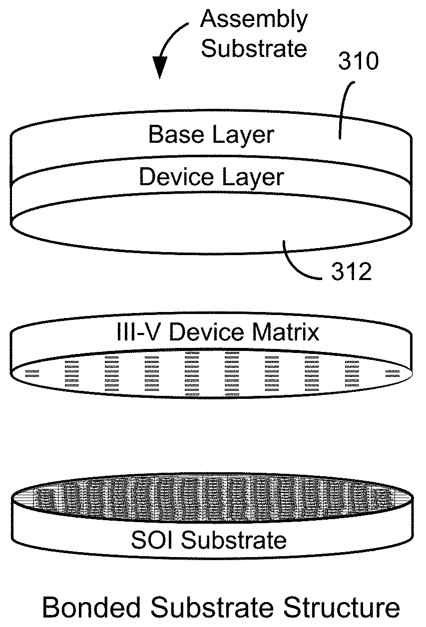
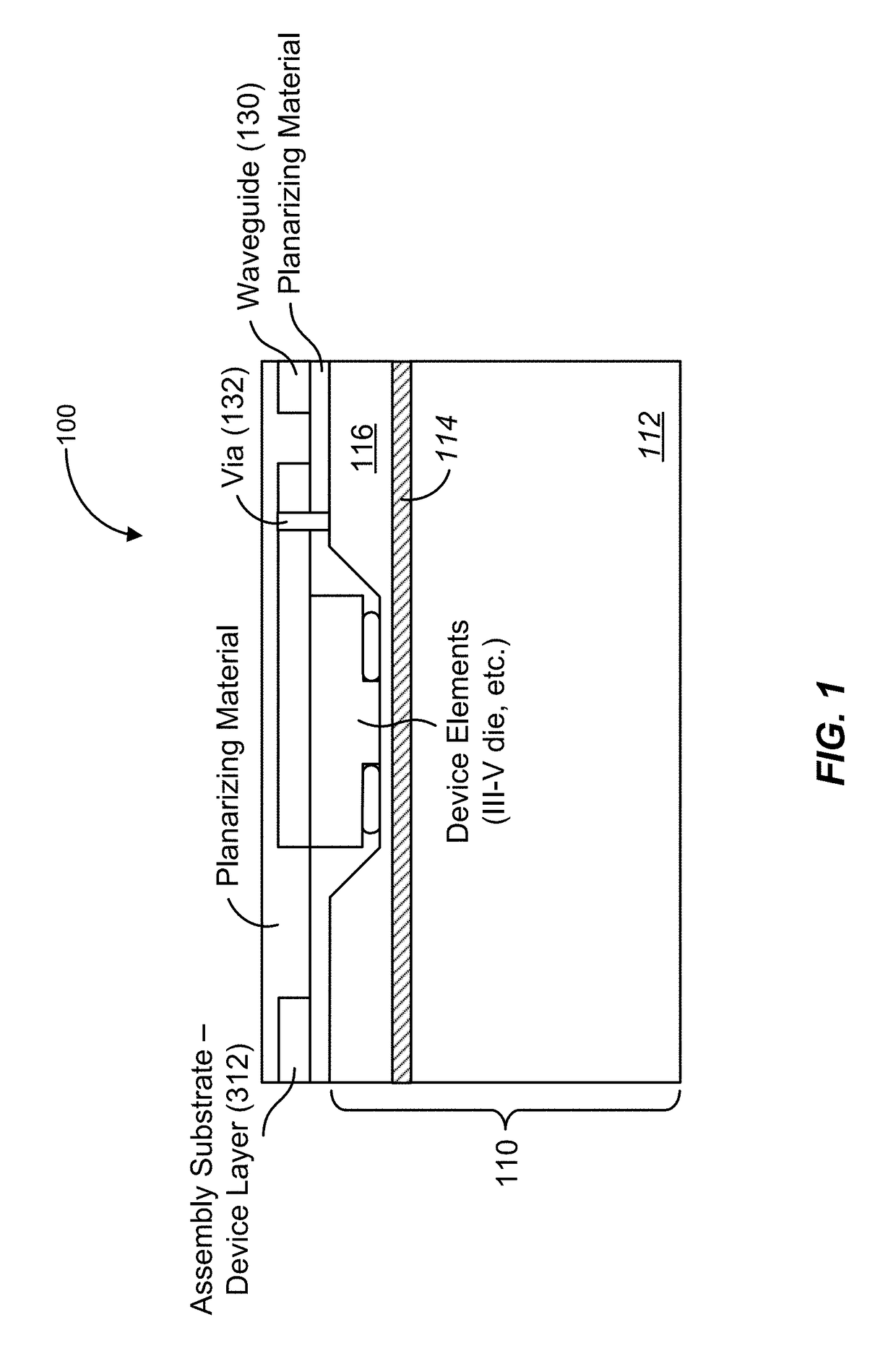
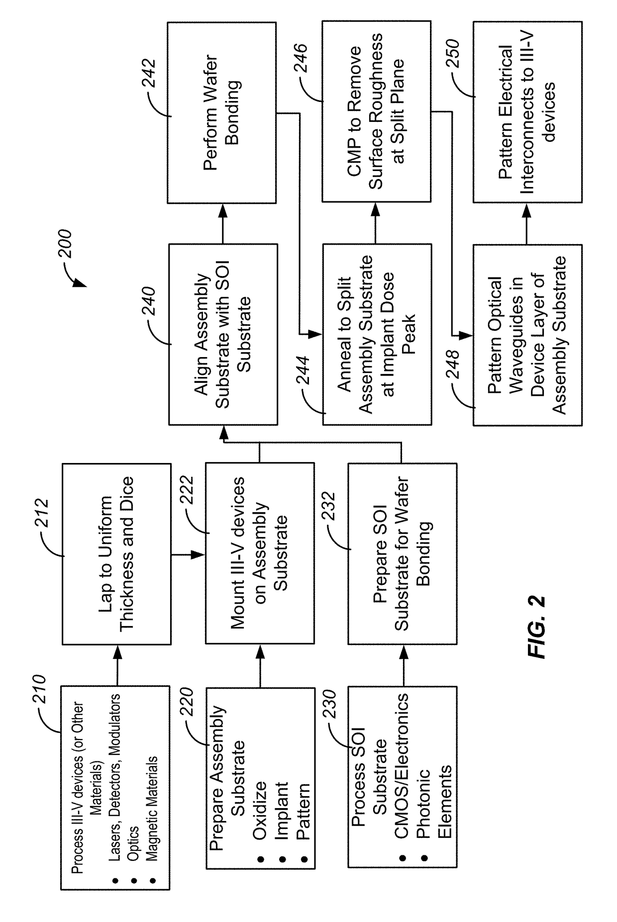
[0034]According to the present invention, methods and systems related to template assisted bonding of semiconductor wafers are provided. Merely by way of example, the invention has been applied to a method of bonding III-V dies (or device regions for more complex circuits) to a substrate at a wafer level using an assembly substrate (also referred to as a template wafer). The method and apparatus is applicable to a variety of semiconductor processing applications including wafer-scale processing of photonics integrating silicon-devices and silicon circuits integrating high-speed electronic functions with compound semiconductor devices.

[0035]The inventors have determined that the commercial significance of silicon photonics will be enhanced if cost and power can be reduced relative to discrete implementations while not sacrificing performance. According to embodiments of the present invention, performance parity is achieved by integrating III-V materials onto the silicon photonic wafe...


PUM


Abstract

Fabricating a multilevel composite semiconductor structure includes providing a first substrate comprising a first material; dicing a second substrate to provide a plurality of dies; mounting the plurality of dies on a third substrate; joining the first substrate and the third substrate to form a composite structure; and joining a fourth substrate and the composite structure.

Description

CROSS-REFERENCES TO RELATED APPLICATIONS[0001]This application is a continuation-in-part of U.S. patent application Ser. No. 14 / 261,276, filed on Apr. 24, 2014, entitled “Method and System for Template Assisted Wafer Bonding Using Pedestals,” which is a continuation of U.S. patent application Ser. No. 13 / 733,337, filed on Jan. 3, 2013, entitled “Method and System for Template Assisted Wafer Bonding Using Pedestals,” now U.S. Pat. No. 8,735,191, issued on May 27, 2014, which claims priority to U.S. Provisional Patent Application No. 61 / 583,095, filed on Jan. 4, 2012, entitled “Method and System for Template Assisted Wafer Bonding Using Pedestals.” This application is also a continuation-in-part of U.S. patent application Ser. No. 14 / 245,191, filed on Apr. 4, 2014, entitled “Method and System for Template Assisted Wafer Bonding,” which is a continuation of U.S. patent application Ser. No. 13 / 869,408, filed on Apr. 24, 2013, entitled “Method and System for Template Assisted Wafer Bondi...

Claims


Application Information

Patent Timeline
Patent Type & Authority Patents(United States)
IPC IPC(8): H01L25/16H01L31/18H01L21/762H01L21/8258G02B6/13H01L21/84H01L21/74H01L25/00H01L21/48H01S5/022H01L33/00H01S5/02
CPCH01L25/50G02B6/13H01L21/4857H01L21/746H01L21/76251H01L21/8258H01L21/84H01L31/18H01S5/0224H01L25/167H01L33/0079H01L2224/16225H01L2224/18H01L2924/0002H01S5/021H01S5/0215H01L2924/00H01L2224/04105H01L2224/73259H01L2224/73267H01L2224/92244H01L2224/92224H01L21/76254H01L2224/24H01L2224/82G02B6/43G02B2006/12061H01L33/0093H01S5/0234G02B6/00
Inventor KRASULICK, STEPHEN B.
Owner SKORPIOS TECH
Why Eureka
Try Eureka