Optical apparatus and methods of manufacture thereof

a technology of optical apparatus and manufacturing methods, applied in the field of optical apparatus, can solve the problems of narrow spectral bandwidth, poor insertion loss of grating couplers, and relatively small mode field diameters

Active Publication Date: 2020-06-30
INTEL CORP
View PDF10 Cites 3 Cited by
  • Summary
  • Abstract
  • Description
  • Claims
  • Application Information

AI Technical Summary

Benefits of technology

[0009]The use of a glass or amorphous material in one embodiment as the first substrate 22 may provide at least one of: improved performance, manufacturability and compatibility with photonic integrated circuit (PIC) platforms. PIC platforms and silica may have similar thermal expansion coefficients, and may be considered to be reliable and / or mechanical stable. The possibility to use 3D laser-inscribed waveguides may provide design freedoms (e.g. by utilizing the third dimension), which may improve performance and / or ease of manufacturability.
[0010]Embodiments described herein may have improved alignment tolerances compared with other approaches. The evanescent coupling approach may provide lower polarization dependence compared with other approaches. The optical apparatus may be relatively straightforward to manufacture and / or may not require any form of polishing in certain embodiments.
[0011]In some embodiments, the first waveguide may be coupled to an optical fiber (e.g. a standard optical fiber, or the like). In spite of the potentially different optical mode sizes of the optical fiber and the second waveguide, the design of the first waveguide may be such that at least one of: low insertion losses, broad spectral bandwidth transmission, low polarization dependence and relaxed alignment tolerances may be achieved.
[0012]By providing a curved section in the first waveguide, the evanescent field in the coupling region may be increased compared with non-curved waveguides. The curved section may provide improved optical coupling efficiency between the first and second waveguides compared with other methods for coupling optical signals between different waveguides. The curved section may allow the resulting evanescent field to propagate over a sufficient distance to permit additional layers to be provided between the first and second waveguides compared with if no curved section is provided. The distance of propagation facilitated by the curved section may allow the first waveguide to be inscribed in the first substrate proximal to the interface without, in some embodiments, necessarily forming part of the interface.
[0051]The further waveguide may allow fabrication of compact photonic components with substantially higher refractive index contrast compared with solely the laser inscribed first waveguide and the second waveguide, as described herein. The optical apparatus may benefit from low loss coupling to the laser-inscribed first waveguide for further integration and low loss interfacing to optical fibers. Example applications may include the fabrication of wavelength multiplexer / demultiplexer circuits on the surface waveguide layers, which may be too large to fabricate with the lower refractive index contrast available with other laser inscribed waveguides, or the like.
[0053]One possible application of using the further waveguide may be to act as an intermediate layer in evanescently coupling to high refractive index contrast platforms. In one example, the further waveguide may help to efficiently transfer the light from the first waveguide into a high refractive index contrast second waveguide. This approach may provide for high coupling efficiencies. Design simulations indicate that total evanescent coupling efficiencies may be above 95%.

Problems solved by technology

The high refractive index contrast of these platforms tends to result in relatively small mode field diameters compared with optical fibers which deliver light into and from the platform.
However, grating couplers suffer from poor insertion losses, have a narrow spectral bandwidth and are restrictive in terms of the polarization of the optical signal.
In use, the optical apparatus may be configured to route an optical signal across the interface, for example, as part of a transceiver or other communication apparatus in which different optical characteristics in different parts of the transceiver or other communication apparatus may otherwise cause issues in terms of inefficient coupling of the optical signal therebetween.

Method used


Image

  • Optical apparatus and methods of manufacture thereof
  • Optical apparatus and methods of manufacture thereof
  • Optical apparatus and methods of manufacture thereof

Examples


Embodiment Construction

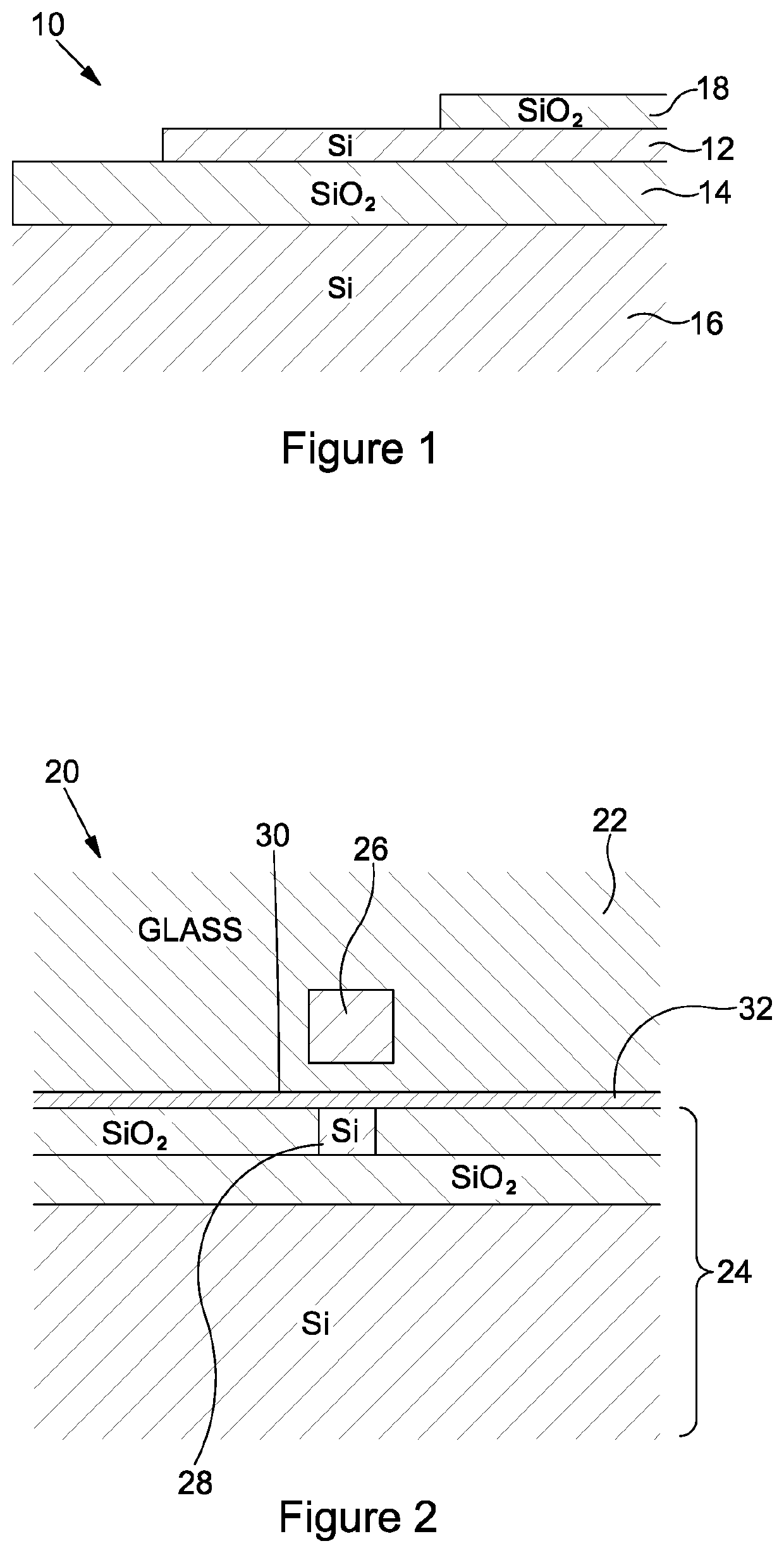
[0118]FIG. 1 shows a cross-sectional schematic view of a photonic integrated circuit (PIC) platform 10. In this embodiment, the PIC platform 10 is in the form of silicon-on-insulator (SOI) structure. The PIC platform 10 comprises a silicon layer 12 on top of an underlayer 14 formed of SiO2 (silica) deposited on top of a bulk substrate 16 comprising silicon. The silicon layer 12 provides a high refractive index contrast optical waveguide. A cladding material (in this embodiment, SiO2) 18 is deposited on the silicon layer 12. In this example, the silicon layer 12 is 220 nm thick and the underlayer 14 is 2 μm thick. It will be appreciated that any appropriate materials may be used for the PIC platform 10 and the particular configuration, number of layers and layer thicknesses may be varied as appropriate.

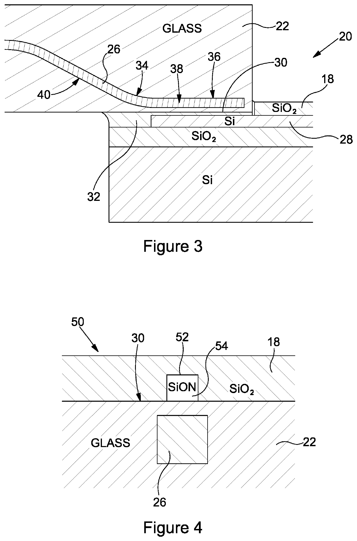
[0119]FIG. 2 shows a first cross-sectional schematic view of an optical apparatus 20 integrated with the PIC platform 10 of FIG. 1. The optical apparatus 20 comprises a first substrate...


PUM

PropertyMeasurementUnit
thickaaaaaaaaaa
thickaaaaaaaaaa
dimensionsaaaaaaaaaa

Abstract

An optical apparatus 20 for evanescently coupling an optical signal across an interface 30 is described. The optical apparatus 20 comprises a first substrate 22 and a second substrate 24. The optical signal is evanescently coupled between a first waveguide 26 formed by laser inscription of the first substrate 22 and a second waveguide 28 of the second substrate 22. The first waveguide 26 comprises a curved section 34 configured to provide evanescent coupling of the optical signal between the first and second waveguides 26, 28 via the interface 30.

Description

FIELD[0001]Described embodiments relate to optical apparatus for routing optical signals, for example but not exclusively in, data communications, and methods of manufacture of such optical apparatus.BACKGROUND[0002]High refractive index contrast photonic integrated circuits (PICs) have applications for use as transceivers for telecommunications. PICs are typically made using platforms such as silicon or indium phosphide. Challenges exist in terms of coupling light efficiently into and out of the PICs with acceptable alignment tolerances, broad bandwidth and low polarization dependence. The high refractive index contrast of these platforms tends to result in relatively small mode field diameters compared with optical fibers which deliver light into and from the platform. The conversion efficiency between dissimilar mode sizes affects the overall coupling performance.[0003]Two possible approaches to providing the optical coupling include grating couplers and edge couplers. Grating co...

Claims


Application Information

Patent Timeline
Patent Type & Authority Patents(United States)
IPC IPC(8): G02B6/12G02B6/13G02B6/125G02B6/293G02B6/42G02B6/122G02B6/30
CPCG02B6/13G02B6/125G02B6/29331G02B6/12002G02B2006/12038G02B6/4231G02B2006/12142G02B2006/12095G02B2006/12061G02B6/4214G02B6/4239G02B2006/12147G02B6/4212G02B6/1223G02B6/305G02B6/1228G02B6/124
Inventor PSAILA, NICHOLAS D.TRAYNOR, ANTHONYPOCOCK, ROWANMITCHELL, PAULBROWN, GRAEMEHESKETH, MARK
Owner INTEL CORP
Why Eureka
Try Eureka