Array substrate and display device

a technology of array substrate and substrate, applied in the field of array substrate and display device, to achieve the effect of improving the quality of the array substrate product and ensuring the performance of the thin film transistor

Active Publication Date: 2018-03-20
BOE TECH GRP CO LTD +1
View PDF14 Cites 0 Cited by
  • Summary
  • Abstract
  • Description
  • Claims
  • Application Information

AI Technical Summary

Benefits of technology

[0008]In view of the above problem existing in the prior art, a technical problem to be solved by the present invention is to provide an array substrate and a display device, thin film transistors in a non-display area and a display area in the array substrate all have bent portions that are at least partially the same in shape, and thus have the same trench exposure performance between the sources and the drains thereof, thereby achieving better display quality.
[0021]The beneficial effects of the present invention are as follows: in the array substrate, since the trenches of the thin film transistors in the non-display area and the display area all have bent portions that are at least partially the same in shape, the exposure of photoresist can be more even during formation of source and drain electrodes by using a patterning process, and thus, the problem of photoresist residues at the trench between the source and the drain due to poor exposure can be avoided; accordingly, defective etching of the trench between the source and the drain due to poor exposure can be avoided in a subsequent etching process for forming a pattern including the source and the drain so as to form the trench between the source and the drain, thereby ensuring performance of the thin film transistors and improving quality of the array substrate product.

Problems solved by technology

It can be seen that, it has become an urgent technical problem to standardize structures of thin film transistors in the non-display area and the display area so as to ensure that the thin film transistors having different structures in the above two areas have a same performance for exposing the trenches between the sources and the drains thereof during an patterning process.

Method used


Image

  • Array substrate and display device
  • Array substrate and display device
  • Array substrate and display device

Examples


embodiment 1

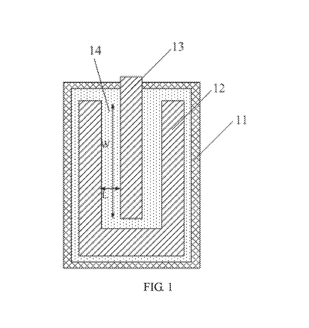
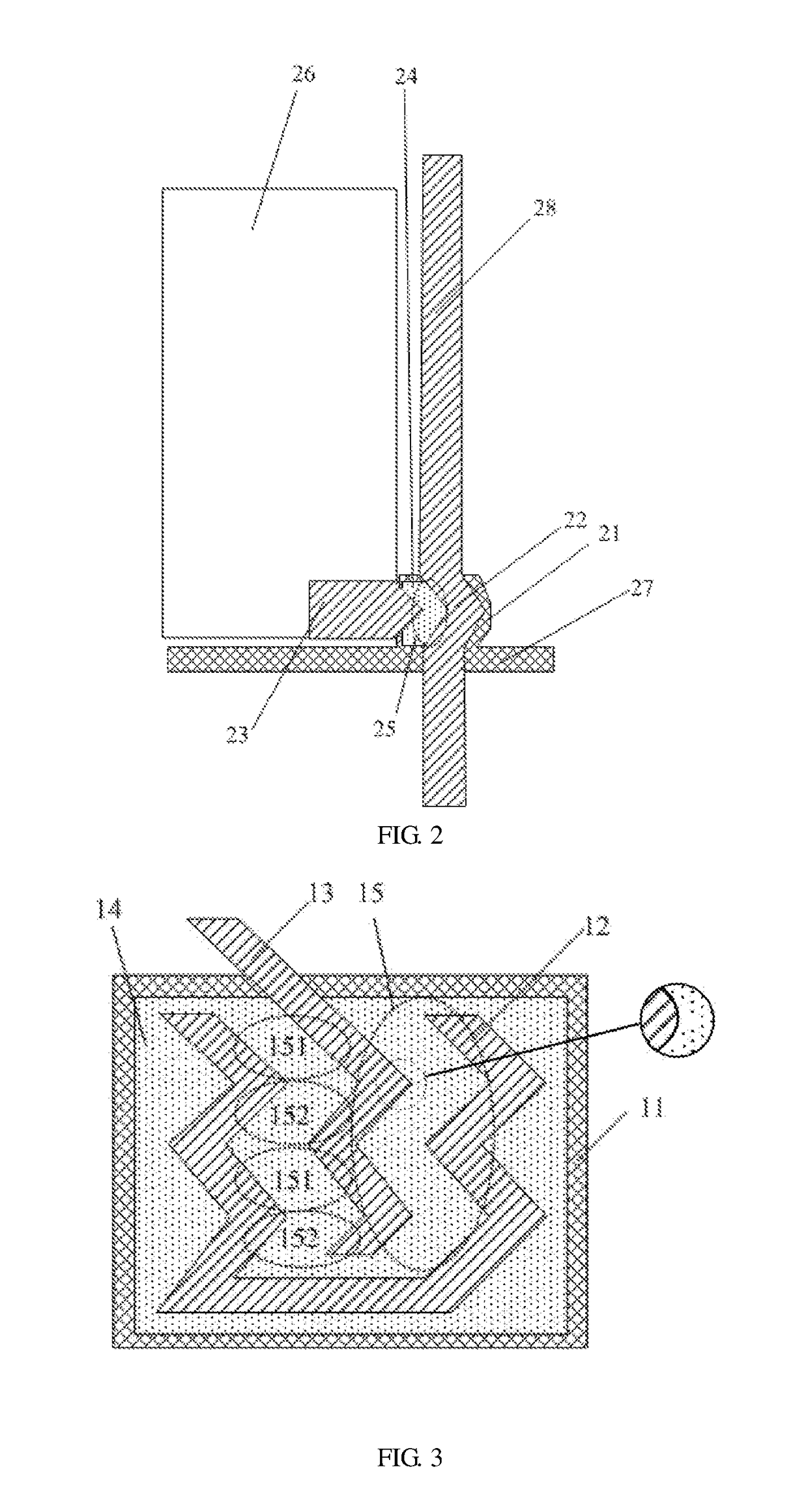
[0032]This embodiment provides an array substrate, in which trenches between sources and drains of thin film transistors in both a display area and a non-display area are set to be at least partially the same in shape, so that exposure difference caused in an exposing step in a patterning process is greatly reduced, and non-uniform exposure is avoided, thereby ensuring performance of the thin film transistors and improving yield and performance of array substrates.

[0033]The concept of the present invention is not limited to the specific exemplary forms in the embodiments, for example, the trenches between the sources and the drains of the thin film transistors in the display area and the non-display area may have any other shape than V-shape, as long as the trench (first trench) in the non-display area and the trench (second trench) in the display area have geometrically similar shapes, and can have same or similar exposure performance.

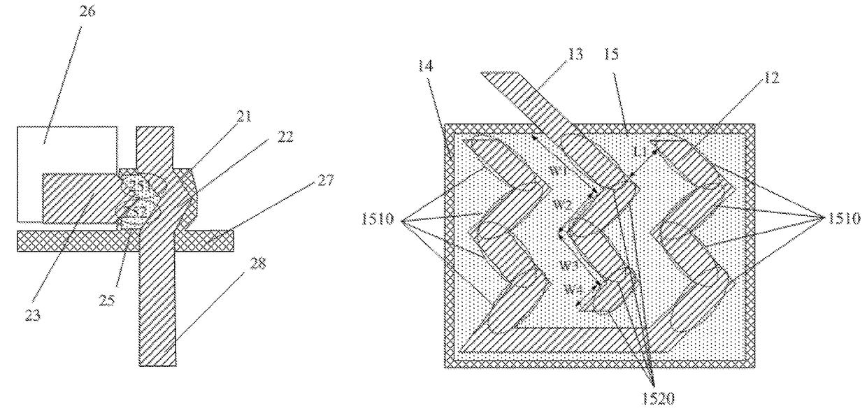
[0034]As shown in FIGS. 3 to 5, the array subst...

embodiment 2

[0052]This embodiment provides a display device, comprising the array substrate in Embodiment 1.

[0053]The display device may be any product or component having a display function, such as a liquid crystal panel, an electronic paper, an OLED panel, a mobile phone, a tablet computer, a television, a display monitor, a notebook computer, a digital photo frame, a GPS or the like.

[0054]The display device uses the above array substrate and thus has a good display quality.


PUM

PropertyMeasurementUnit
bending anglesaaaaaaaaaa

Abstract

The present invention relates to an array substrate and a display device. The array substrate comprises a first thin film transistor arranged on a non-display area of the array substrate and a second thin film transistor arranged on a display area of the array substrate, a part of a first active layer corresponding to a region between a first source and a first drain in the first thin film transistor forms a first trench, and a part of a second active layer corresponding to a region between a second source and a second drain in the second thin film transistor forms a second trench, the first trench has at least one first bent portion, the second trench has a second bent portion, and bending angles of the first bent portion and the second bent portion are the same or explementary angles.

Description

[0001]This is a National Phase Application filed under 35 U.S.C. 371 as a national stage of PCT / CN2016 / 070097, filed Jan. 5, 2016, an application claiming the benefit of Chinese Application No. 201510393988.7, filed Jul. 7, 2015, the content of each of which is hereby incorporated by reference in its entirety.FIELD OF THE INVENTION[0002]The present invention relates to the field of display technology, and particularly, relates to an array substrate and a display device.BACKGROUND OF THE INVENTION[0003]In a tablet display device, thin film transistors (TFTs) arranged in matrix and a driving chip for driving the thin film transistors are generally provided on an array substrate, in order to control every pixel. In general, the thin film transistors are formed in a display area by a patterning process, and the driving chip is bonded in a non-display area.[0004]With the development of display technology, GOA (Gate on Array) technique has been developed, that is, a gate driving circuit i...

Claims


Application Information

Patent Timeline
Patent Type & Authority Patents(United States)
IPC IPC(8): H01L27/32H01L27/12G02F1/1362G02F1/1368H01L29/786H01L29/417
CPCH01L27/3262H01L27/124H01L27/3276H01L27/1251H01L27/1222G02F1/1368H01L27/12G02F1/13454H10K59/1213H10K59/131
Inventor WANG, JINGHE, WEI
Owner BOE TECH GRP CO LTD
Why Eureka
Try Eureka