Flash memory structure and fabrication method thereof
a technology of flash memory and fabrication method, which is applied in the direction of semiconductor devices, electrical apparatus, transistors, etc., can solve the problems of reducing the electrical properties and reliability of the semiconductor structure, affecting the interconnection of processes, and reducing the spacing between the devices
- Summary
- Abstract
- Description
- Claims
- Application Information
AI Technical Summary
Benefits of technology
Problems solved by technology
Method used
Image


Examples
Embodiment Construction
[0013]Reference will now be made in detail to exemplary embodiments of the invention, which are illustrated in the accompanying drawings. Wherever possible, the same reference numbers will be used throughout the drawings to refer to the same or the alike parts.
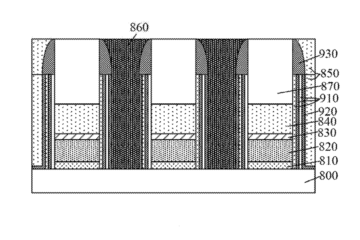
[0014]When the NOR flash memory is formed by existing techniques, a contact-hole plug needs to be formed at both sides of a gate structure to connect to a source region and / or a drain region. FIGS. 1-3 illustrate flash memory structures corresponding to certain stages of an existing fabrication process of a flash memory structure. Referring to FIG. 1, the fabrication process includes providing a substrate 100, and forming a gate structure 110 on the substrate 100 and a hard mask layer 120 on top of the gate structure. The hard mask layer 120 is configured as an etching mask for forming the gate structure 110. The fabrication process also includes forming a sidewall structure 130 on side surfaces of the gate structure 110 and t...
PUM
| Property | Measurement | Unit |
|---|---|---|
| temperature | aaaaa | aaaaa |
| time | aaaaa | aaaaa |
| thickness | aaaaa | aaaaa |
Abstract
Description
Claims
Application Information