Organic light emitting diode display device including pixel driving circuit

a light-emitting diode and display device technology, applied in the direction of static indicating devices, instruments, etc., can solve the problems of data voltage deviation, voltage difference between anodes, pixels may have different driving tft threshold voltages, etc., to suppress luminance drops, minimize leakage current, and minimize voltage differences

Active Publication Date: 2018-04-24
LG DISPLAY CO LTD
View PDF19 Cites 3 Cited by
  • Summary
  • Abstract
  • Description
  • Claims
  • Application Information

AI Technical Summary

Benefits of technology

[0009]The present disclosure is conceived to solve the above-described problem. In the present disclosure, an apparatus comprising a circuit configured to control anode voltages of one or more adjacent pixel rows, which are adjacent to an Nth pixel row, to achieve minimal voltage differences between said Nth pixel row and said adjacent pixel rows to suppress luminance drops in an OLED display by minimizing leakage currents being introduced from adjacent pixel rows. The circuit configured to set said anode voltages of said one or more adjacent pixel rows to be equal to or less than an anode voltage of said Nth pixel row when said Nth pixel row is operating in a sampling period or in a programming period among driving operation periods of said OLED display.second scan signal

Problems solved by technology

However, while the OLED display device writes data to the first pixel row through the lowermost pixel row in order, there is a time when a voltage difference is generated between anodes of adjacent pixels.
Such a data voltage deviation caused by the leakage current becomes a big problem when a resistance of the common single layer decreases.
Meanwhile, in the OLED display device, a problem occurs as pixels may have different driving TFT threshold voltages Vth and mobility due to process variation.
Further, a voltage drop of a high-potential voltage VDD occurs, causing an amount of current driving the OLED to be changed.

Method used


Image

  • Organic light emitting diode display device including pixel driving circuit
  • Organic light emitting diode display device including pixel driving circuit
  • Organic light emitting diode display device including pixel driving circuit

Examples


Embodiment Construction

[0023]Hereinafter, an OLED display device and a method for driving the same according to an exemplary embodiment of the present disclosure will be described in detail with reference to the accompanying drawings.

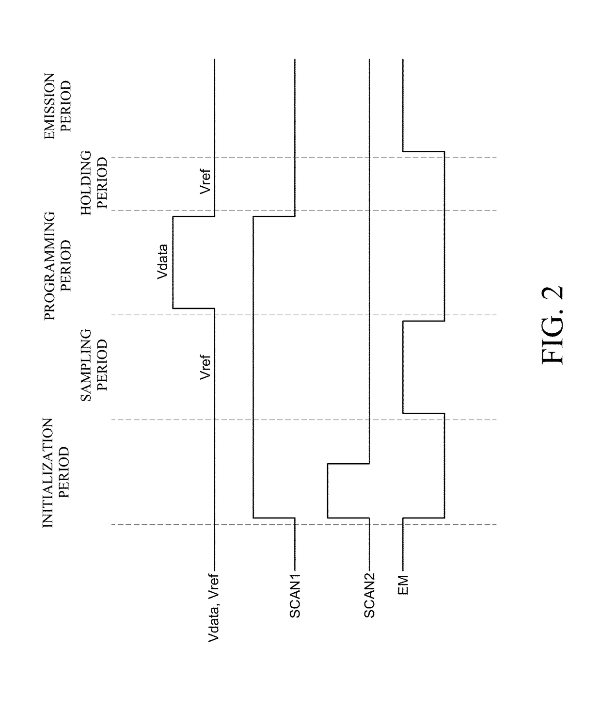
[0024]A thin film transistor (TFT) employed in the present disclosure may be of a P type or an N type. In the following exemplary embodiment, there will be described a case where a TFT is of an N type, for convenience in explanation. In this regard, a gate high voltage VGH is a gate-on voltage to turn on a TFT, and a gate low voltage VGL is a gate-off voltage to turn off a TFT. In explaining pulse type signals, a gate high voltage (VGH) state is defined as a “high state”, and a gate low voltage (VGL) state is defined as a “low state”.

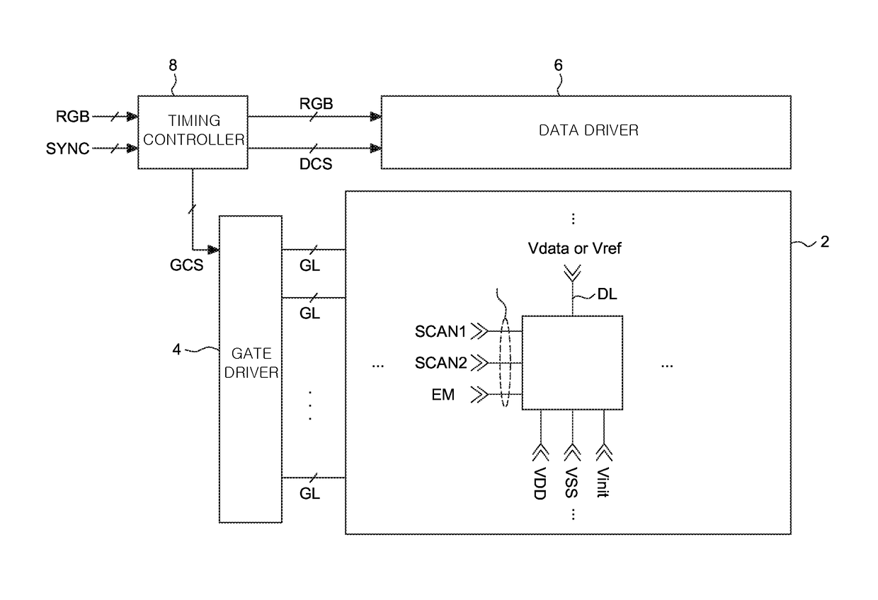
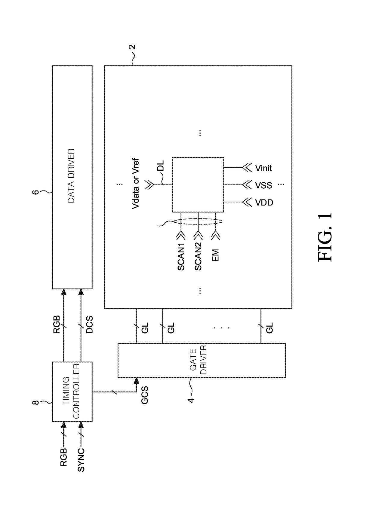
[0025]FIG. 1 is a configuration view of an OLED display device according to an exemplary embodiment of the present disclosure.

[0026]As illustrated in FIG. 1, the OLED display device includes a display panel 2 including a plurality of pixels P def...


PUM


Abstract

An apparatus comprising a circuit configured to control anode voltages of one or more adjacent pixel rows, which are adjacent to an Nth pixel row, to achieve minimal voltage differences between said Nth pixel row and said adjacent pixel rows to suppress luminance drops in an OLED display by minimizing leakage currents being introduced from adjacent pixel rows.

Description

CROSS-REFERENCE TO RELATED APPLICATIONS[0001]This application claims the priority of Korean Patent Application No. 10-2014-0084053 filed on Jul. 4, 2014, in the Korean Intellectual Property Office, the disclosure of which is incorporated herein by reference.BACKGROUND[0002]Technical Field[0003]The present disclosure relates to an organic light emitting diode (hereinafter, referred to as “OLED”) display device.[0004]Description of the Related Art[0005]Each of a plurality of pixels constituting an OLED display device includes an OLED having an organic light emitting layer between an anode and a cathode and a pixel circuit that independently drives the OLED. The pixel circuit includes a switching thin film transistor (hereinafter, referred to as “TFT”), a capacitor, and a driving TFT. The switching TFT charges the capacitor with a data voltage in response to a scan pulse. The driving TFT regulates emission of the OLED by controlling the amount of current supplied to the OLED according ...

Claims


Application Information

Patent Timeline
Patent Type & Authority Patents(United States)
IPC IPC(8): G09G3/30G09G3/3291G09G3/3233
CPCG09G3/3291G09G3/3233G09G2300/0819G09G2320/0223G09G2300/0861G09G2310/0256G09G2320/0214G09G2300/0852
Inventor YOON, SANGHUNKANG, CHANGHEONLEE, JUNGMIN
Owner LG DISPLAY CO LTD
Why Eureka
Try Eureka