Memory architecture with multi-bank memory cell array accessed by local drive circuit within memory bank

a memory cell array and memory bank technology, applied in the memory field, can solve the problems of increasing the area and the cost of memory dies, and achieve the effect of high bandwidth data access and high speed random access

Active Publication Date: 2018-06-12
PIECEMAKERS TECH
View PDF8 Cites 0 Cited by
  • Summary
  • Abstract
  • Description
  • Claims
  • Application Information

AI Technical Summary

Benefits of technology

[0004]It is therefore one objective of the present invention to provide a circuit architecture and a latch-type local drive circuit so that memories can share a global address decoder circuit, thus greatly reducing influence of memory die areas to realize an architecture having multiple independent sets of memory banks.
[0006]The proposed memory architecture may provide a plurality of memory banks in one memory cell array, wherein the memory banks can be accessed independently of each other according to a shared address decoder circuit (e.g. including a global column select decoder and / or a global memory section decoder) by employing a latch-type local drive circuit (e.g. including a column select drive circuit and / or a sense amplifier drive circuit), thereby achieving high bandwidth data access and high speed random access.

Problems solved by technology

However, in a case where a conventional memory device having multiple memory banks is utilized to perform data access, as different memory banks need respective column select decoders and respective bit line sense amplifier control signals, areas and costs of memory dies increase greatly.

Method used


Image

  • Memory architecture with multi-bank memory cell array accessed by local drive circuit within memory bank
  • Memory architecture with multi-bank memory cell array accessed by local drive circuit within memory bank
  • Memory architecture with multi-bank memory cell array accessed by local drive circuit within memory bank

Examples


Embodiment Construction

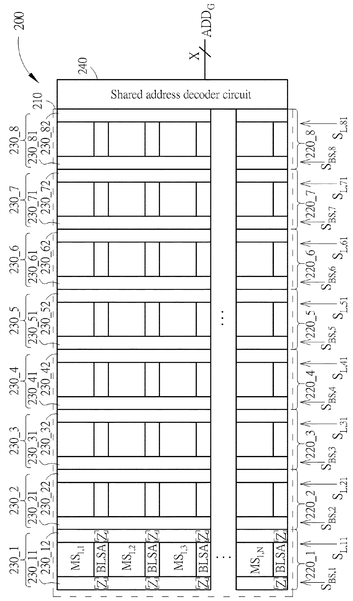
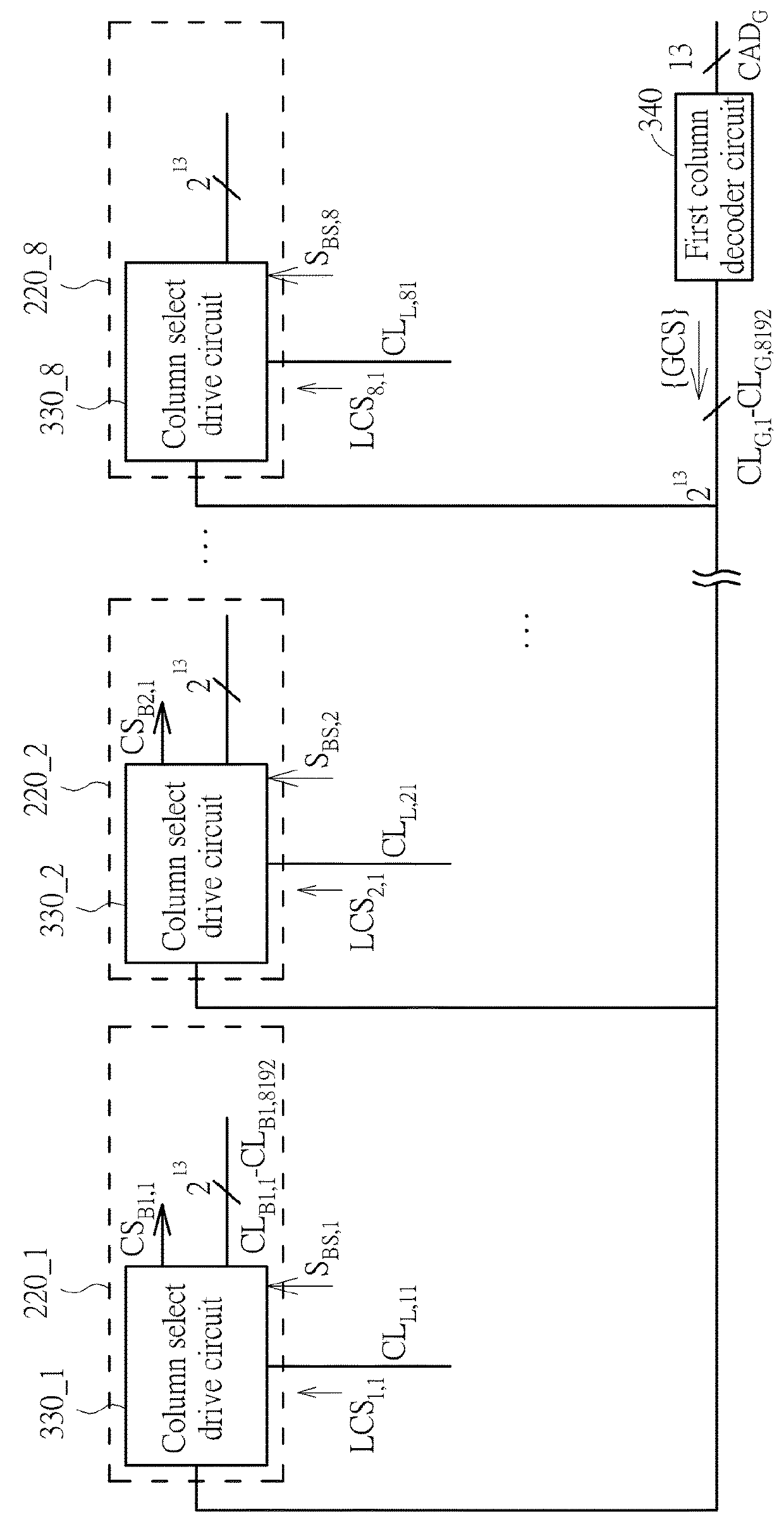
[0021]To provide flexible data access mechanism, the proposed memory architecture may employ a hierarchical column driving structure to access a plurality of memory banks included within a memory cell array, wherein the memory banks may be accessed independently in an interleaved sequence according to a shared global signal, respective memory bank select signals and respective local signals, and each memory bank select signal may enable the shared global signal to be applied to a corresponding memory bank. Further description is provided below.

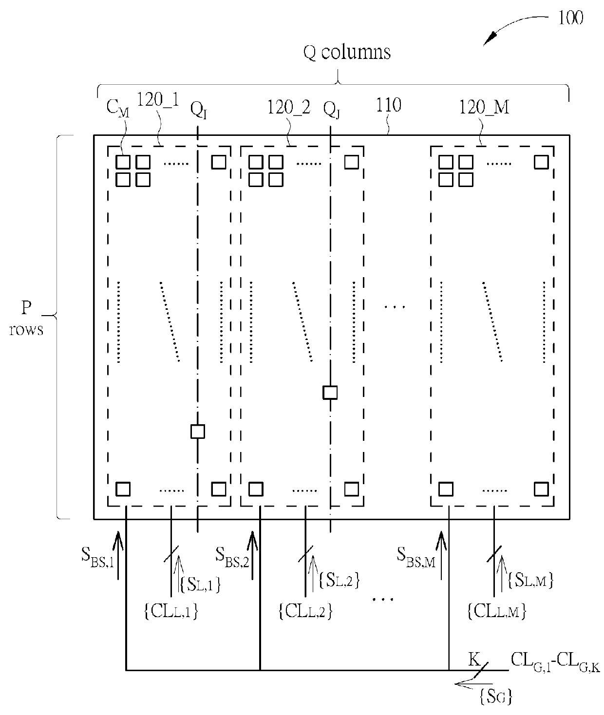
[0022]Please refer to FIG. 1, which is a diagram illustrating an exemplary memory architecture according to an embodiment of the present invention. The memory architecture 100 may include, but is not limited to, a memory cell array 110 which includes a plurality of memory cells arranged in P rows and Q columns (P and Q are positive integers), wherein each memory cell is labeled CM. Each memory cell may be disposed in correspondence with an int...


PUM


Abstract

A memory architecture includes K first control lines, M groups of second control lines and a memory cell array. K and M are positive integers. Each group of second control lines includes at least one second control line. The memory cell array includes M memory banks. Each memory bank is coupled to the K first control lines. The M memory banks are selected according to M bank select signals respectively so as to receive a shared set of first control signals through the K first control lines. The M memory banks are coupled to the M groups of second control lines respectively, and receive independent M sets of second control signals through the M groups of second control lines respectively. Each memory bank performs one of a column select operation and a sense amplification operation according to the set of first control signals and a set of second control signals.

Description

CROSS REFERENCE TO RELATED APPLICATIONS[0001]This application claims the benefit of U.S. provisional application No. 62 / 384,164, filed on Sep. 6, 2016, the contents of which are incorporated herein by reference.BACKGROUND OF THE INVENTION1. Field of the Invention[0002]The disclosed embodiments of the present invention relate to memory, and more particularly, to a memory architecture including a memory cell array divided into multiple memory banks which can be accessed independently of each other according to a shared address decoder.2. Description of the Prior Art[0003]A conventional memory bank has its own independent / dedicated column select decoders (or bit switches) and bit line sense amplifier control signals to perform data access. However, in a case where a conventional memory device having multiple memory banks is utilized to perform data access, as different memory banks need respective column select decoders and respective bit line sense amplifier control signals, areas and...

Claims


Application Information

Patent Timeline
Patent Type & Authority Patents(United States)
IPC IPC(8): G11C7/22G11C7/06G11C8/10G11C7/12G11C8/12
CPCG11C8/12G11C8/10G11C7/12G11C7/065G11C7/18
Inventor WANG, MING-HUNGWANG, GYH-BINTING, TAH-KANG JOSEPH
Owner PIECEMAKERS TECH
Why Eureka
Try Eureka