High-speed, low power, medium resolution analog-to-digital converter and method of stabilization

a technology of analog-to-digital converter and medium resolution, applied in the field of analog-to-digital converter, can solve the problems of large integrated circuit area, high power consumption, and increase of all such requirements, and achieve the effect of cancelling out input offset voltages

Inactive Publication Date: 2002-05-28
MARVELL ASIA PTE LTD
View PDF18 Cites 24 Cited by
  • Summary
  • Abstract
  • Description
  • Claims
  • Application Information

AI Technical Summary

Benefits of technology

Accordingly, the full flash ADC of the present invention includes a plurality of comparators and a referencing scheme that effectively cancels out the input offset voltages of the comparators. The input offset voltage of each of the plurality of comparators is obtained by performing a self calibration process on the ADC during, for example, power up. Then, the input offset voltage for each of the comparators is stored in a look-up table. When the ADC is used, the look-up table provides offset correction to the normal reference voltages for each comparator.

Problems solved by technology

ADCs for operation at high frequencies, however, require a large amount of integrated circuit area and have high power consumption, and all such requirements increase as the number of bit of resolution of the ADC increases.
Unfortunately, such two-phase design limits the maximum achievable operating frequency to a factor of two lower than otherwise possible, other factors being equal, if non-auto zero voltage comparators are employed.
Non-auto zero voltage comparators, such as those used in full flash ADCs implemented in Bipolar or BiCMOS integrated circuit processes, are generally not practical for implementation in standard CMOS processes because device mismatches (e.g., input offset voltage) of CMOS voltage comparators tend to be much higher than for Bipolar equivalents.
CMOS voltage comparators with low input offset voltage can usually only be obtained using complex circuitry that requires large integrated circuit area with associated higher power consumption, and generally lower conversion speed.

Method used


Image

  • High-speed, low power, medium resolution analog-to-digital converter and method of stabilization
  • High-speed, low power, medium resolution analog-to-digital converter and method of stabilization
  • High-speed, low power, medium resolution analog-to-digital converter and method of stabilization

Examples


Embodiment Construction

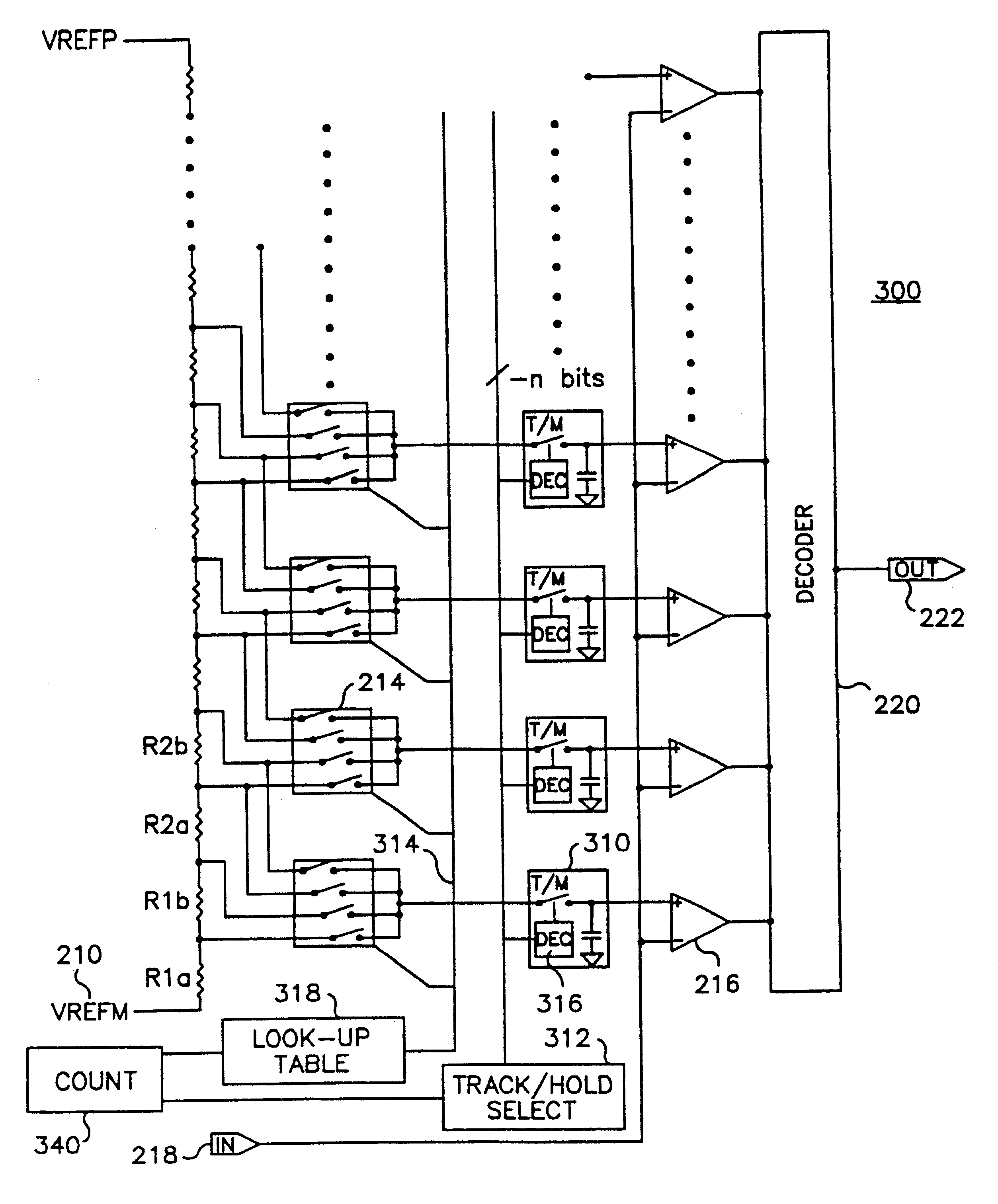
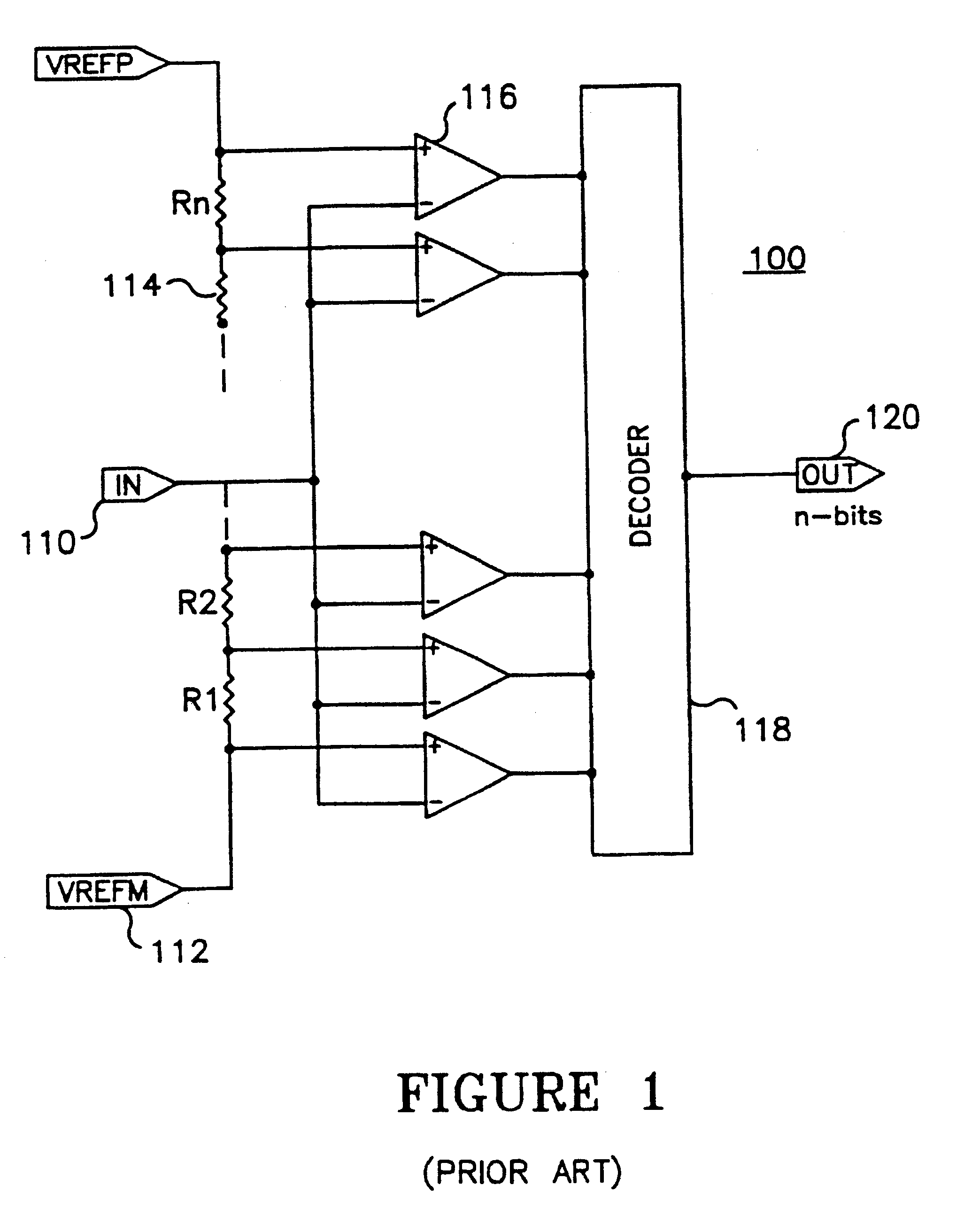
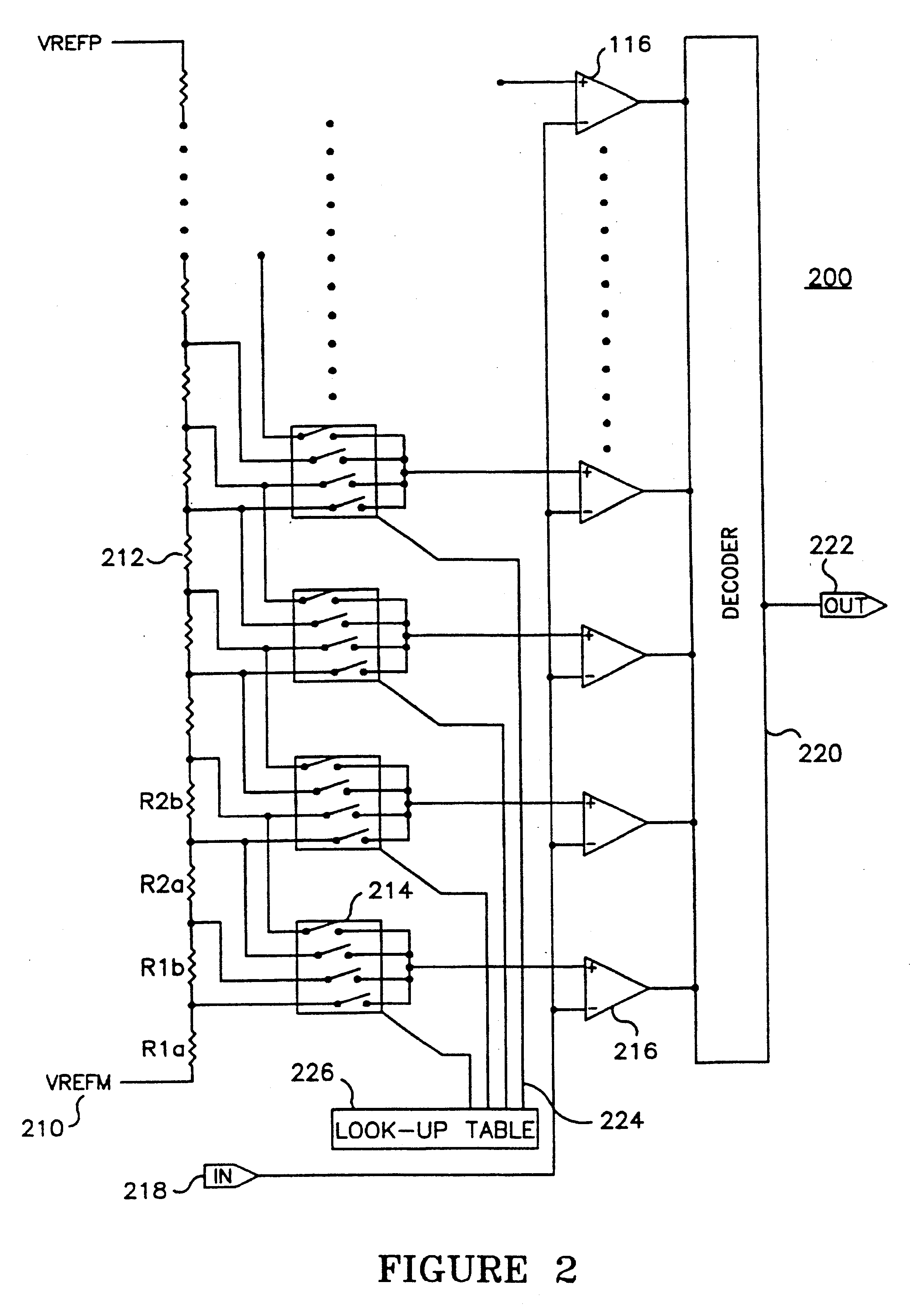
FIG. 2 is a block diagram of a calibrated analog-to-digital converter ("ADC") 200 having four choices of reference voltage per comparator derived from a reference voltage input 210. A number of resistors, of which resistor 212 is exemplary, are coupled in series to the reference voltage 210. A number of switching circuits, of which switching circuit 214 is exemplary, are coupled to junctions of resistors 212 to apply selected ones of four different voltages to a reference input of each comparator 216. The output of each switching circuit 214 is coupled to an associated comparator, of which comparator 216 is exemplary. In addition, each comparator 216 receives an input voltage appearing on input 218. A conventional decoder 220 receives the outputs of the comparators 216 and produces a digital output 222 representation of the voltage appearing on input 218.

The embodiment of a full flash ADC 200 illustrated in FIG. 2 includes an array of comparator 216 arranged to receive associated re...


PUM


Abstract

A full flash analog to digital converter operates on an input voltage with a track/hold circuit coupled to a reference input of each of multiple comparators. Particular track/hold circuits are activated in sequence through a track/hold select circuit, and a look-up table and a digital-to-analog converter are coupled to supply corrected reference voltages to each track/hold circuit. Outputs of the comparators are supplied to a decoder which produces the digital output representative of the input voltage. The converter is calibrated before it is used for conversion by sensing the input offset voltages of each of the comparators and by altering the reference voltage for each comparator to produce a calibrated reference voltage for each comparator. A digital representation of the calibrated reference voltage for each comparator is stored in a look-up table for retrieval as needed to supply to a particular track/hold circuit a corresponding calibrated analog reference voltage for a particular comparator. Digital representations in the look-up table may indicate switch settings required to provide corrected reference voltages, or may indicate the required corrected reference voltage that is supplied by digital to analog converter which converts the digital representation into an analog corrected reference voltage that is held by the track/hold circuit. In this manner, each track/hold circuit is loaded with its respective calibrated reference voltage. An input signal applied to each comparator triggers such comparators upon parity between the corrected reference voltage and input voltage, and all comparator outputs are supplied to a decoder which produces a digital representation of the input signal. Occasionally, the entries in the look-up table and each track/hold circuit may be refreshed or updated in order to compensate for drift of the calibrated reference voltage.

Description

FIELD OF INVENTIONThis invention pertains in general to analog-to-digital converters and in particular to analog-to-digital converters having a very high operating clock frequency, small die size, and low power consumption and methods of stabilizing the same against drift.BACKGROUND OF THE INVENTIONConventional high-speed analog-to-digital converters ("ADCs") commonly employ a full flash architecture in which the analog-to-digital conversion is done in parallel by using approximately 2.sup.n voltage comparators. FIG. 1 illustrates a conventional full flash ADC 100 including an input voltage 110, a reference voltage 112, a number of resistors, of which resistor 114 is representative, a number of conventional comparators, of which comparator 116 is representative, and a conventional decoder 118 that produces a multi-bit digital output 120.As is well known in the art, input voltage 110 is applied simultaneously to each comparator 116. In addition, fractional portions of the reference v...

Claims


Application Information

Patent Timeline
Patent Type & Authority Patents(United States)
IPC IPC(8): H03M1/10H03M1/36
CPCH03M1/1061H03M1/365
Inventor SUTARDJA, SEHATSUTARDJA, PANTAS
Owner MARVELL ASIA PTE LTD
Why Eureka
Try Eureka