Masks for use in optical lithography below 180 nm

Inactive Publication Date: 2006-10-17
ROCHESTER INSTITUTE OF TECHNOLOGY
View PDF8 Cites 0 Cited by
  • Summary
  • Abstract
  • Description
  • Claims
  • Application Information

AI Technical Summary

Benefits of technology

[0012]The present invention provides a number of advantages including providing a mask which has desirable optical properties for use in optical lithography at or below about 180 nm. More specifically, the mask has an optical density of at least 4.0 for wavelengths at or below about 180 nm with a thickness equal to or less than about 1000 angstroms.
[0013]The present invention also provides a mask with suitable etch characteristics. The layer of masking material can be etched without a significant loss of the underlying substrate or resist material.

Problems solved by technology

The challenge is in finding a material or materials for use as the mask which will satisfy these requirements.
However, as shown in FIG. 1, chromium metal is a less desirable choice as a mask for wavelengths below 193 nm.
At these optical densities, mask modulation is likely to be low for imaging of fine feature geometry.
Unfortunately, a masking film thickness of over about 800 Å is undesirable for 157 nm applications because of the aspect ratio requirements of features smaller than 300 nm.

Method used


Image

  • Masks for use in optical lithography below 180 nm
  • Masks for use in optical lithography below 180 nm
  • Masks for use in optical lithography below 180 nm

Examples


Embodiment Construction

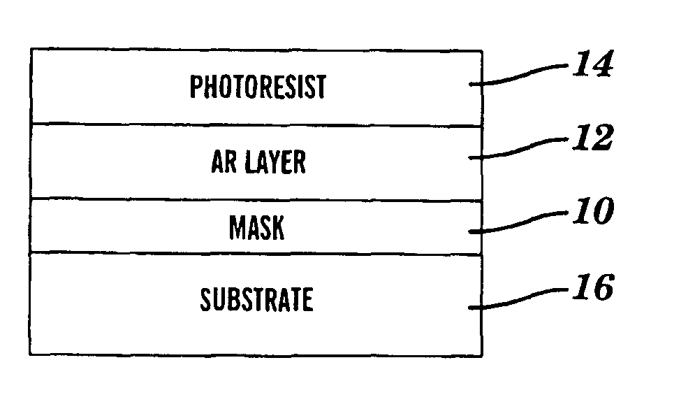
[0024]A mask film 10 for use in optical lithography at or below about 180 nm in accordance with one embodiment of the invention as illustrated in FIG. 10. The mask 10 has an optical density of at least about 4.0 for wavelengths at or below about 180 nm and a thickness of about 1000 angstroms or less. The present invention provides a number of advantages including providing a mask 10 which has suitable optical properties for lithography at or below about 180 nm and has suitable etch characteristics.

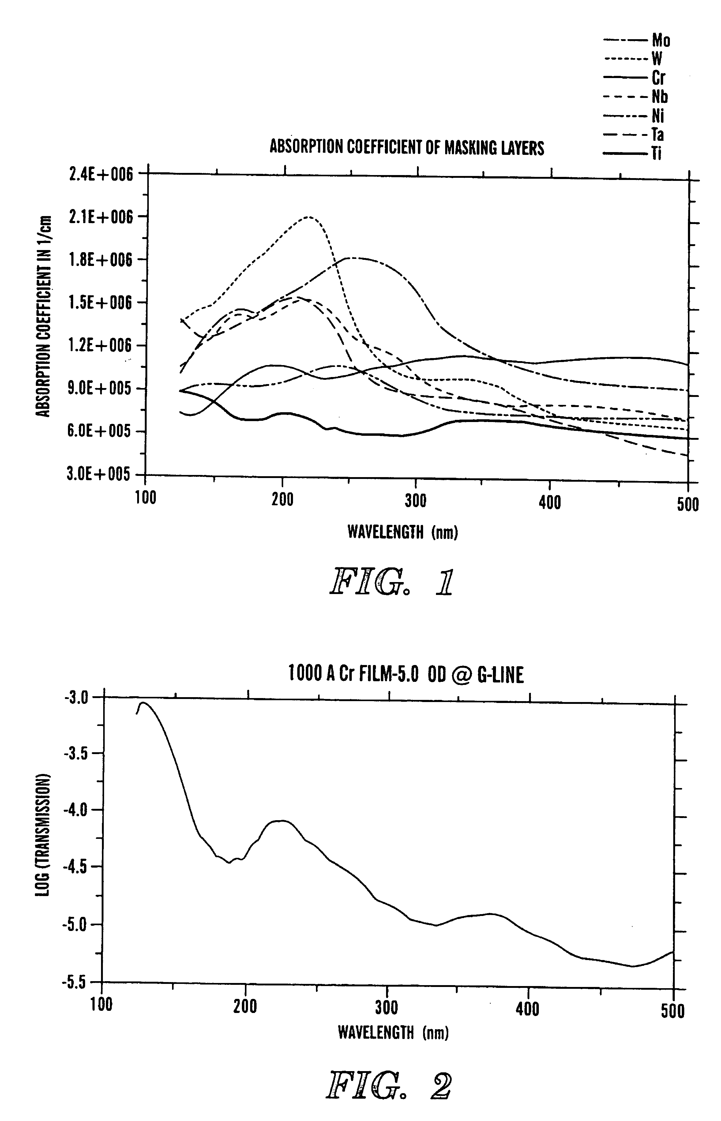
[0025]Referring to FIG. 1, the absorption coefficients (1 / cm) for molybdenum (Mo), tungsten (W), chromium (Cr), niobium (Nb), nickel (Ni), tantalum (Ta), and titanium (Ti) metals at wavelengths from 110 nm to 500 nm are illustrated. As discussed in greater detail earlier in the background with reference to FIGS. 1 and 2, chromium is a good choice for use as a mask 10 for wavelengths ranging between about 193 nm to about 436 nm, but does not possess desirable optical properties as a mask 10...


PUM


Abstract

A mask for use on a layer of imaging material which is located on at least a portion of one surface of a substrate in a lithography process in accordance with one embodiment of the present invention includes a layer of a masking material which has an optical density of at least 4.0 for wavelengths at or below about 180 nm and a thickness of less than about 1000 angstroms. Materials, such as tungsten and amorphous silicon, can be used for the mask.

Description

[0001]This application claims the benefit of U.S. Provisional Patent Application Ser. No. 60 / 118,795 filed on Feb. 5, 1999 which is herein incorporated by reference.FIELD OF THE INVENTION[0002]This invention relates generally to lithography and, more particularly, to masks for use in optical lithography at or below about 180 nm.BACKGROUND OF THE INVENTION[0003]Lithography is a process for producing a pattern on a semiconductor wafer. The pattern is produced by first exposing a pattern etched into a mask onto a semiconductor wafer coated with a resist material. The projected image of the pattern changes the composition of the resist material on the semiconductor wafer which is then removed to leave a matching pattern on the semiconductor wafer for further processing.[0004]Depending upon the particular lithography application, the mask needs to satisfy several different requirements. The challenge is in finding a material or materials for use as the mask which will satisfy these requi...

Claims


Application Information

Patent Timeline
IPC IPC(8): G01F9/00G03F1/00G03F1/54G03F7/09
CPCG03F1/50G03F1/54G03F7/091
Inventor SMITH, BRUCE W.
Owner ROCHESTER INSTITUTE OF TECHNOLOGY
Why Eureka
Try Eureka